Methods for sidewall protection of metal interconnect for unlanded vias using physical vapor deposition

a metal interconnect and physical vapor deposition technology, applied in the direction of semiconductor/solid-state device manufacturing, basic electric elements, electric devices, etc., can solve the problems of less uniform deposition and unlanded nature, and achieve the effect of less expensive sidewall protection

Inactive Publication Date: 2005-11-01
SEMICON COMPONENTS IND LLC
View PDF6 Cites 22 Cited by
  • Summary
  • Abstract
  • Description
  • Claims
  • Application Information

AI Technical Summary

Benefits of technology

[0012]The foregoing problems with the prior state of the art are overcome by the principles of the present invention, which are directed towards methods for protecting the sidewall of a metal interconnect component using Physical Vapor Deposition (PVD) processes and using a single barrier metal material, thereby allowing for less expensive sidewall protection.

Problems solved by technology

Physical Vapor Deposition typically results in a less uniform deposition, particularly on the side walls.
The unlanded nature of the via is not necessarily (and is probably not) by design, but is expected to occur due to alignment difficulties.

Method used


Image

  • Methods for sidewall protection of metal interconnect for unlanded vias using physical vapor deposition
  • Methods for sidewall protection of metal interconnect for unlanded vias using physical vapor deposition
  • Methods for sidewall protection of metal interconnect for unlanded vias using physical vapor deposition

Examples


Embodiment Construction

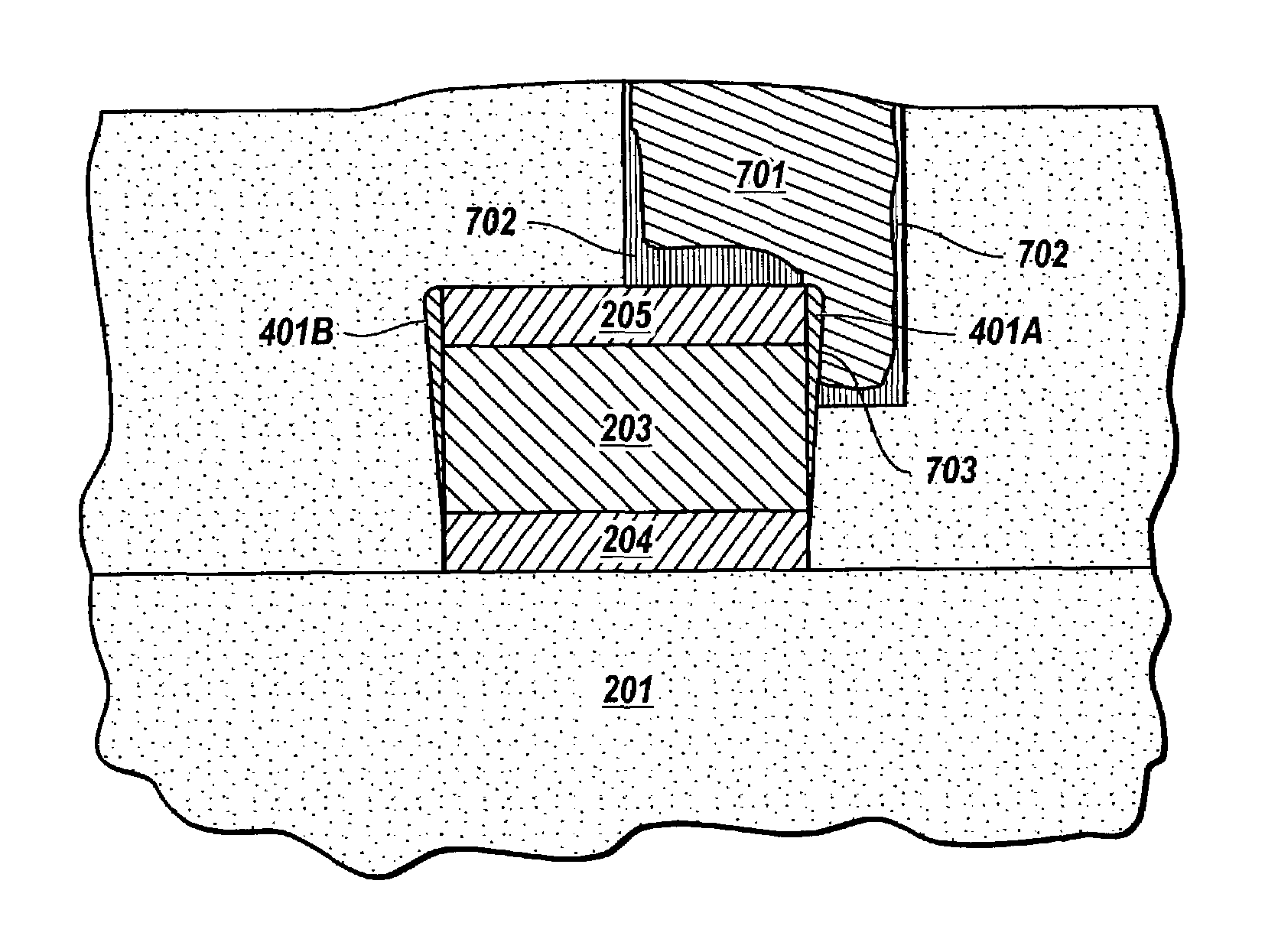
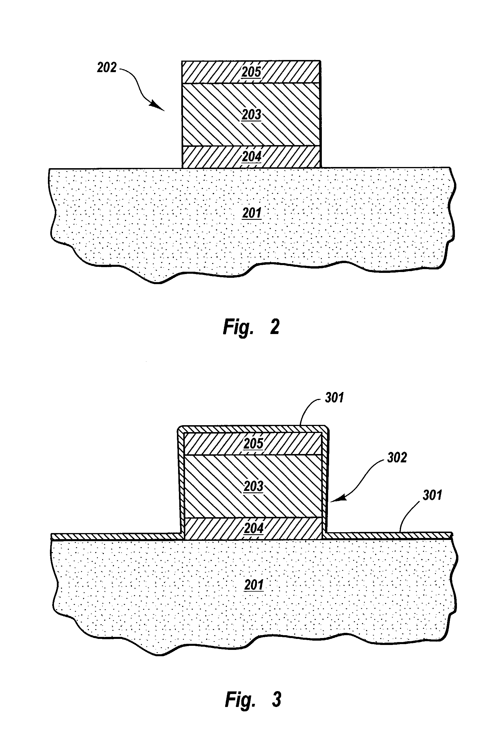
[0027]The principles of the present invention involve methods for protecting the sidewall of a metal interconnect component using Physical Vapor Deposition (PVD) processes and using a single barrier metal material, thereby allowing for less expensive sidewall protection. After forming the metal interconnect component, a single barrier metal is deposited on at least a portion of a sidewall of the metal interconnect component using a Physical Vapor Deposition (PVD) process such as sputtering. A subsequent anisotropic etching of the barrier metal removes the barrier metal from the horizontal surface except for some that still remains on the top surface of the metal interconnect layer. The barrier metal deposited through PVD on vertical surfaces substantially remains. A dielectric layer is then formed over the metal interconnect component and the barrier metal. The unlanded via is etched through the dielectric layer to the metal interconnect component so that the barrier metal that cove...


PUM

PropertyMeasurementUnit
thicknessaaaaaaaaaa
thicknessaaaaaaaaaa
dielectricaaaaaaaaaa

Abstract

Methods for protecting the sidewall of a metal interconnect component using Physical Vapor Deposition (PVD) processes and using a single barrier metal material. After forming the metal interconnect component, a single barrier metal is deposited on its sidewall using PVD. A subsequent anisotropic etching of the barrier metal removes the barrier metal from the horizontal surface except for some that still remains on the top surface of the metal interconnect layer. A dielectric layer is then formed over the metal interconnect component and the barrier metal. The unlanded via is etched through the dielectric layer to the metal interconnect component, and then filled with a second metal to thereby allow the metal interconnect component to electrically connect with one or more upper metal layers.

Description

BACKGROUND OF THE INVENTION[0001]1. The Field of the Invention[0002]The present invention relates to semiconductor device fabrication technology, and more specifically, to methods for protecting the sidewall of a metal interconnect during a subsequent plug fill of an unlanded via.[0003]2. Background and Related Art[0004]Computing technology has revolutionized the way people work and play and has contributed enormously to the advancement of humankind. Much of computing technology has been enabled by the discovery and advancement of semiconductor processing technology.[0005]Semiconductor processing technology allows for the formation of highly integrated circuits with multiple metal layers. By constructing integrated circuits with multiple metal layers, a given circuit with given feature dimension sizes may be fabricated using much less space than it would if it was permitted just a single metal layer. Furthermore, multiple metal layers enables for much more efficient design and opera...

Claims


Application Information

Patent Timeline
Patent Type & Authority Patents(United States)
IPC IPC(8): H01L21/02H01L21/311H01L21/768
CPCH01L21/76852
Inventor NELSON, MARK M.WILLIAMS, BRETT N.PRASAD, JAGDISH
Owner SEMICON COMPONENTS IND LLC
Why Eureka
Try Eureka