Semiconductor device having a gate structure surrounding a fin

a technology of semiconductor and gate structure, which is applied in the direction of semiconductor devices, transistors, electrical devices, etc., can solve the problems of short channel effect, increased difficulty in overcoming, and reduced design features below 100 nm, so as to achieve the effect of increasing the total channel width

Active Publication Date: 2005-11-01
ADVANCED MICRO DEVICES INC
View PDF7 Cites 22 Cited by
  • Summary
  • Abstract
  • Description
  • Claims
  • Application Information

AI Technical Summary

Benefits of technology

[0005]Implementations consistent with the present invention provide a FinFET device with a gate structure that surrounds a conductive fin. By having gate material surround the fin, the FinFET device has an increased total channel width as compared to conventional FinFET devices.

Problems solved by technology

The reduction of design features below 100 nm challenges the limitations of conventional methodology.
For example, when the gate length of conventional planar metal oxide semiconductor field effect transistors (MOSFETs) is scaled below 100 nm, problems associated with short channel effects, such as excessive leakage between the source and drain, become increasingly difficult to overcome.
In addition, mobility degradation and a number of process issues also make it difficult to scale conventional MOSFETs to include increasingly smaller device features.

Method used


Image

  • Semiconductor device having a gate structure surrounding a fin
  • Semiconductor device having a gate structure surrounding a fin
  • Semiconductor device having a gate structure surrounding a fin

Examples


Embodiment Construction

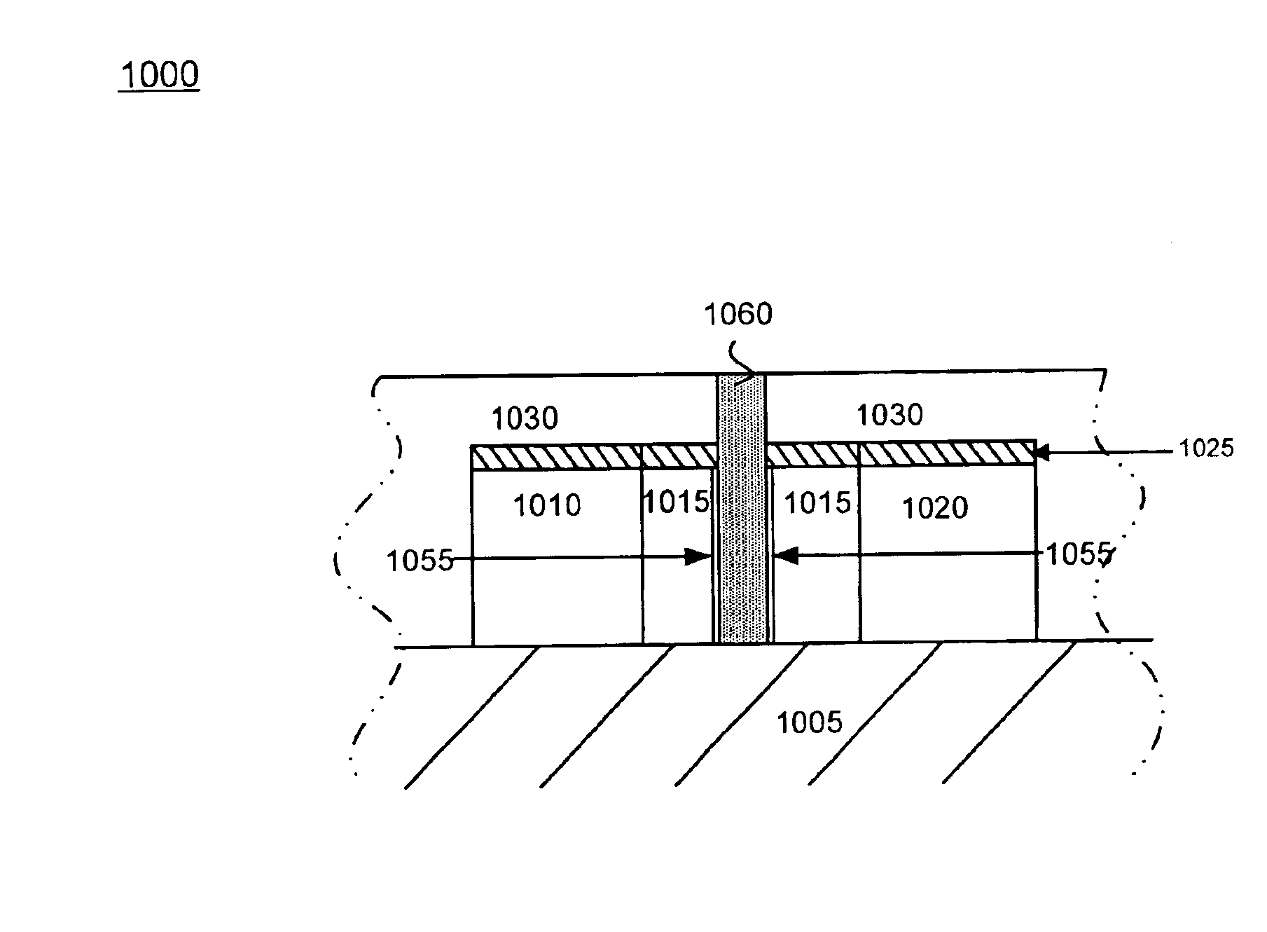
[0024]The following detailed description of the invention refers to the accompanying drawings. The same reference numbers in different drawings may identify the same or similar elements. Also, the following detailed description does not limit the invention. Instead, the scope of the invention is defined by the appended claims and their equivalents.

[0025]Implementations consistent with the present invention provide FinFET devices and methods of manufacturing such devices. The FinFET devices formed in accordance with the present invention include a fin that is surrounded by gate material. The resulting FinFET devices have increased channel width as compared to conventional FinFET devices.

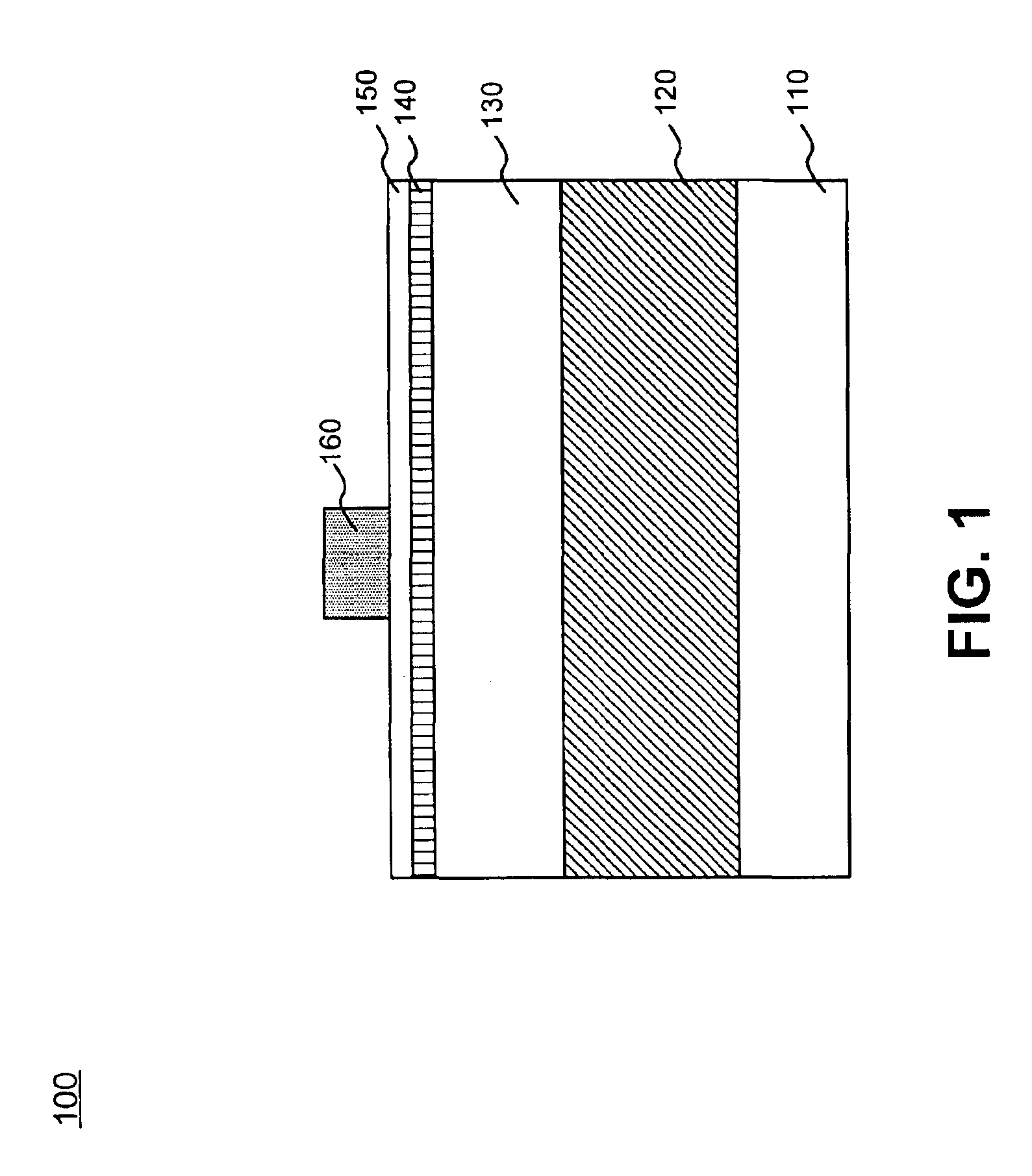
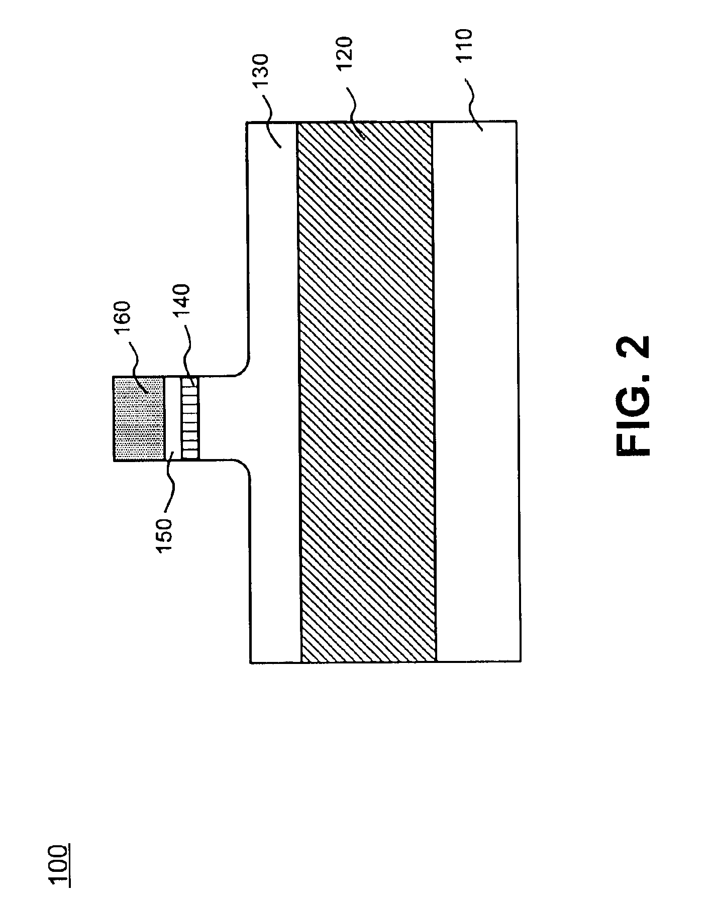
[0026]FIG. 1 illustrates the cross-section of a semiconductor device 100 formed in accordance with an exemplary embodiment of the present invention. Referring to FIG. 1, semiconductor device 100 may include a silicon on insulator (SOI) structure that includes a silicon substrate 110, a buried oxide la...


PUM


Abstract

A double-semiconductor device includes a substrate, an insulating layer, a fin and a gate. The insulating layer is formed on the substrate and the fin is formed on the insulating layer. The fin has a number of side surfaces, a top surface and a bottom surface. The gate is formed on the insulating layer and surrounds the top surface, bottom surface and the side surfaces of the fin in the channel region of the semiconductor device. Surrounding the fin with gate material results in an increased total channel width and more flexible device adjustment margins.

Description

TECHNICAL FIELD[0001]The present invention relates to semiconductor devices and methods of manufacturing semiconductor devices. The present invention has particular applicability to double-gate device.BACKGROUND ART[0002]The escalating demands for high density and performance associated with ultra large scale integration semiconductor devices require design features, such as gate lengths, below 100 nanometers (nm), high reliability and increased manufacturing throughput. The reduction of design features below 100 nm challenges the limitations of conventional methodology.[0003]For example, when the gate length of conventional planar metal oxide semiconductor field effect transistors (MOSFETs) is scaled below 100 nm, problems associated with short channel effects, such as excessive leakage between the source and drain, become increasingly difficult to overcome. In addition, mobility degradation and a number of process issues also make it difficult to scale conventional MOSFETs to incl...

Claims


Application Information

Patent Timeline
Patent Type & Authority Patents(United States)
IPC IPC(8): H01L29/66H01L29/788H01L21/027H01L21/336H01L29/786
CPCH01L29/42392H01L29/66795H01L29/785H01L21/0276
Inventor YANG, CHIH-YUHAHMED, SHIBLY S.AN, JUDY XILINDAKSHINA-MURTHY, SRIKANTESWARAYU, BIN
Owner ADVANCED MICRO DEVICES INC
Why Eureka
Try Eureka