Closed cell configuration to increase channel density for sub-micron planar semiconductor power device

a semiconductor power device and closed cell technology, applied in semiconductor devices, semiconductor device details, electrical apparatus, etc., can solve the problems of not providing an effective solution to reduce the on-resistance of the lateral mosfet device, the vdmos transistor cannot be conveniently integrated, etc., to achieve the effect of increasing the channel width per unit area, increasing the on-resistance, and increasing the channel density

Active Publication Date: 2007-12-27
ALPHA & OMEGA SEMICON LTD
View PDF8 Cites 13 Cited by
  • Summary
  • Abstract
  • Description
  • Claims
  • Application Information

AI Technical Summary

Benefits of technology

[0009]It is therefore an aspect of the present invention to provide a new and improved lateral semiconductor power device implemented with novel layout to increase the channel width per unit area. The on-resistance can be further increased with this novel layout of cell array suitable for large current switching operations such that the above discussed problems and difficulties can be resolved.
[0010]Specifically, it is an aspect of the present invention to provide improved lateral semiconductor power device implemented with a new layout of transistor cells in a transistor cell array. In this new transistor cell array, the gate regions formed generally with polysilicon disposed between the source and drain regions are configured to have a wave-like configuration. The polysilicon gate regions are formed to comply with the minimum spacing rule allowed by the technology. Since the polysilicon gate regions are drawn to a minimum spacing with the source and drain contacts between the polysilicon gates formed with a wave-like pattern, a higher channel density is achieved. A higher channel density translated into a higher channel width per unit area (W / area).
[0011]Briefly in a preferred embodiment this invention discloses a lateral semiconductor power device supported on a semiconductor substrate. The lateral semiconductor power device includes a plurality of transistor cells each includes a source and a drain region disposed on opposite sides of a gate region in the semiconductor substrate wherein a gate electrode is formed as an electrode layer on top of the gate region for controlling an electric current transmitted between the source and the drain regions. The gate electrode layer disposed on top the semiconductor layer is patterned into a wave-shape configuration for substantially increasing an electric current conduction area between the source and drain regions across the gate.
[0012]This invention further discloses a method for configuring a semiconductor power device supported on a semiconductor substrate. The method includes a step of forming a plurality of transistor cells each with a source and a drain region disposed on opposite sides of a gate region in the semiconductor substrate. The method further includes a step of forming a gate electrode layer on top of the gate region on top of the gate region for controlling an electric current transmitted between the source and the drain regions and patterning the gate electrode layer into a wave-shaped stripes for substantially increasing an electric current conduction area between the source and drain regions across the gate.

Problems solved by technology

However, there are applications where the VDMOS transistors cannot be conveniently integrated.
For this reason, with a strong demand to miniaturize the electronic devices, this method does not provide an effective solution to reduce the on-resistance of the lateral MOSFET devices.

Method used


Image

  • Closed cell configuration to increase channel density for sub-micron planar semiconductor power device
  • Closed cell configuration to increase channel density for sub-micron planar semiconductor power device
  • Closed cell configuration to increase channel density for sub-micron planar semiconductor power device

Examples


Embodiment Construction

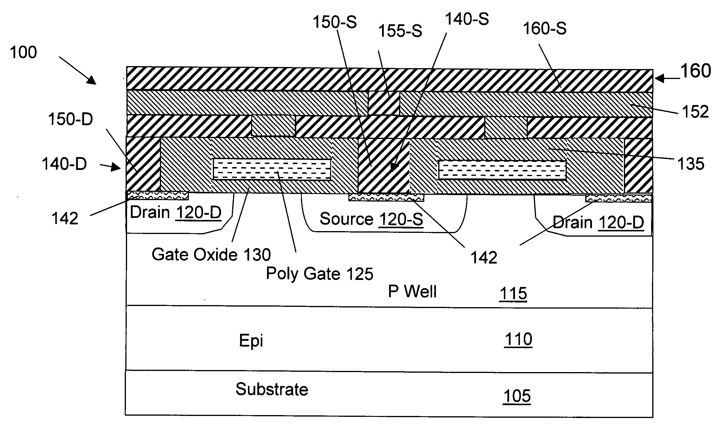
[0018]Referring to FIGS. 2A to 2E for a serial of top views for showing the polysilicon layout in FIG. 2A and the processes in forming contacts and the source, drain and gate metal layers for providing electrical contacts for the lateral semiconductor power device of this invention. FIG. 2F is a side cross sectional view of the lateral semiconductor power transistor cell across line A-A′ in FIG. 2A. As shown in FIGS. 2F and 2A, the lateral semiconductor power device 100 is supported on a semiconductor substrate 105 formed with an epitaxial layer 110 with a P-well 115 formed in the epitaxial layer 110. Alternatively, the P-well 115 may be formed directly on top of substrate 105 without epitaxial layer 110. The semiconductor power transistor cell further includes a source region 120-S and a drain region 120-D with a polysilicon gate 125 disposed on top of a gate oxide layer 130 for controlling a channel between the source and the drain regions. The semiconductor power transistor cell ...


PUM


Abstract

A semiconductor power device supported on a semiconductor substrate that includes a plurality of transistor cells, each cell has a source and a drain region disposed on opposite sides of a gate region in the semiconductor substrate. A gate electrode is formed as an electrode layer on top of the gate region for controlling an electric current transmitted between the source and the drain regions. The gate electrode layer disposed on top of the semiconductor substrate is patterned into a wave-like shaped stripes for substantially increasing an electric current conduction area between the source and drain regions across the gate.

Description

BACKGROUND OF THE INVENTION[0001]1. Field of the Invention[0002]The invention relates generally to the planar semiconductor power devices. More particularly, this invention relates to an improved and novel closed cell configuration with increased channel density, i.e., the channel width per unit of semiconductor area, for sub-micron planar semiconductor power device.[0003]2. Description of the Prior Art[0004]Conventional technologies have reached a limit to reduce the on-resistance of lateral MOS transistors by increasing the channel width in a given MOS transistor area. Reduction of the on-resistance for a cellular array of MOS transistors is desirable because of the lower power loss and ability to conduct high currents. In low voltage application, e.g., MOSFETS application for a voltage lower than 12 volts, lateral MOSFETs offer lower device resistance than vertical double-diffused metal oxide field effect transistors (VDMOS). However, in design large area lateral MOSFETs, the con...

Claims


Application Information

Patent Timeline
Patent Type & Authority Applications(United States)
IPC IPC(8): H01L27/10
CPCH01L27/0207H01L27/088H01L29/4238H01L2924/0002H01L23/52H01L23/528H01L23/535H01L2924/00H01L29/0696H01L29/41758H01L29/7816
Inventor MALLIKARARJUNASWAMY, SHEKAR
Owner ALPHA & OMEGA SEMICON LTD
Why Eureka
Try Eureka