Image sensor and forming method thereof

An image sensor and semiconductor technology, which is applied in the field of image sensors, can solve the problems of pixel unit ratio limitation, increase of low-frequency 1/f noise, and decrease of dynamic range, etc., to achieve quality improvement, strong channel control, and performance improvement Effect

Active Publication Date: 2014-07-16
GALAXYCORE SHANGHAI
View PDF5 Cites 13 Cited by
  • Summary
  • Abstract
  • Description
  • Claims
  • Application Information

AI Technical Summary

Problems solved by technology

Therefore, although the circuits around the pixel array can further reduce the line width and size according to Moore's Law, the transistor devices in the pixel unit can only be reduced very slowly.
The area of ​​the entire image sensor chip is mainly determined by the pixel array. Therefore, the structure of the existing pixel unit limits the further reduction of the chip area, making the cost of the image sensor high.
[0014] 2. In the existing pixel unit, the four transistor devices are all planar structures. For a pixel unit of a certain size, after containing four transistor devices, the size can be further reduced. ratio is limited
In the traditional existing process, even though great effort is spent on these aspects, the ideal effect cannot be achieved because the process limit has been reached. Therefore, new image sensors and corresponding proces

Method used


Image

  • Image sensor and forming method thereof
  • Image sensor and forming method thereof
  • Image sensor and forming method thereof

Examples


Embodiment Construction

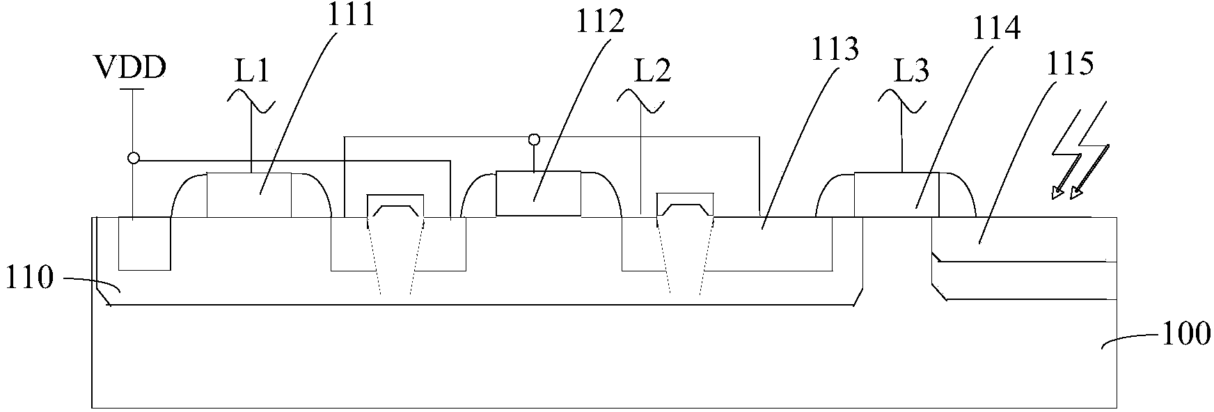
[0066] In existing image sensors, transistors (such as source follower transistors, transfer transistors, and reset transistors, etc.) are usually planar structures. Therefore, the corresponding pixel units have many defects. For example, it is difficult to further reduce the chip area of ​​image sensors. The cost remains high, the image quality formed by the image sensor is difficult to further improve, the noise level of the image sensor is difficult to reduce, and the area occupancy rate of the photoelectric conversion element in the pixel unit is difficult to increase.

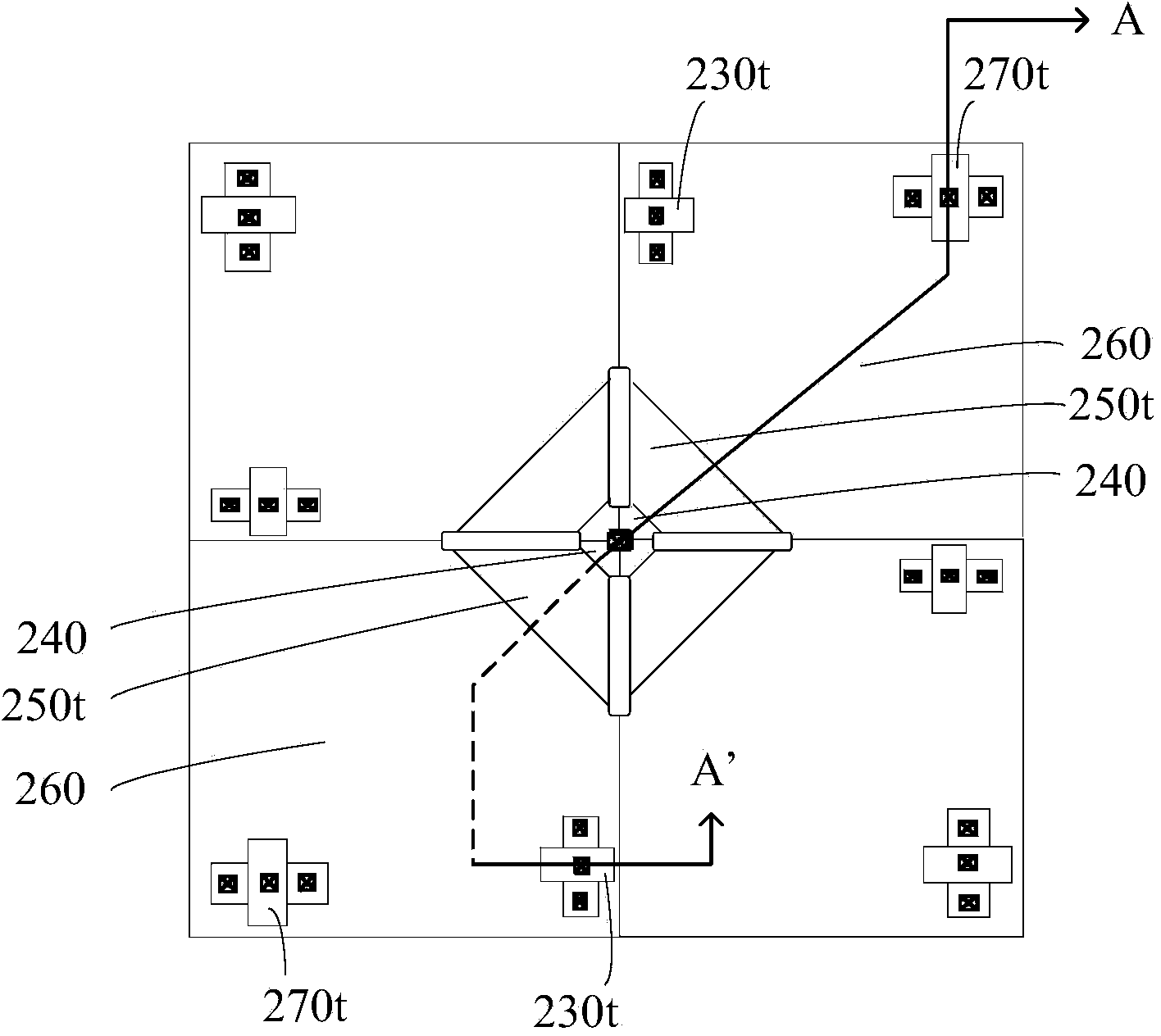
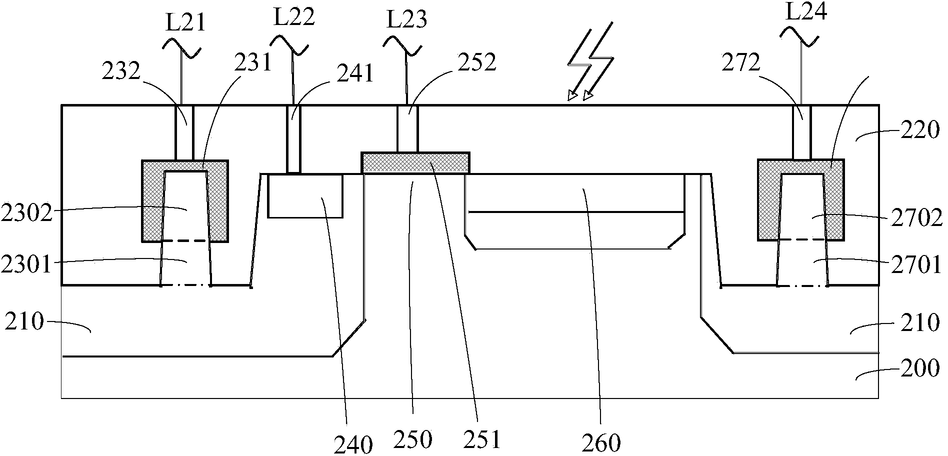
[0067] For this reason, the present invention proposes a kind of image sensor, in the image sensor provided by the present invention, pixel unit has the source follower transistor of three-dimensional structure, so the performance of pixel unit improves, thereby can improve the image quality that image sensor produces, also can At the same time, the performance of the image sensor chip can be improved, and ...


PUM


Abstract

The invention discloses an image sensor and a forming method thereof. The image sensor comprises a pixel array, and the pixel array comprises a plurality of pixel units which are arranged in an array mode. Each pixel unit comprises a semiconductor substrate, a photodiode, a floating diffusion region, a transfer transistor and a source-follower transistor, wherein the photodiode is placed in the semiconductor substrate, the floating diffusion region is placed in the semiconductor substrate, the transfer transistor comprises a source electrode and a drain electrode which are placed in the semiconductor substrate, the source electrode and the drain electrode are electrically connected with a photovoltaic conversion element and the floating diffusion region respectively, the source-follower transistor comprises a grid electrode placed on the semiconductor substrate, the grid electrode is electrically connected with the floating diffusion region, a channel region of the source-follower transistor is of a cross beam structure, the cross beam structure is provided with a top face and two side faces, and the grid electrode of the source-follower transistor covers at least one of the top face and the two side faces. The performance of the image sensor is improved, and cost is lowered.

Description

technical field [0001] The present invention relates to the field of image sensors, in particular to an image sensor and a forming method thereof. Background technique [0002] An image sensor is a semiconductor device that converts an optical signal into an electrical signal, and the image sensor has a photoelectric conversion element. [0003] Image sensors can be further divided into complementary metal oxide (CMOS) image sensors and charge-coupled device (CCD) image sensors. The advantage of the CCD image sensor is that it has high image sensitivity and low noise, but it is difficult to integrate the CCD image sensor with other devices, and the power consumption of the CCD image sensor is relatively high. In contrast, CMOS image sensors have the advantages of simple process, easy integration with other devices, small size, light weight, low power consumption, and low cost. Therefore, with the development of technology, CMOS image sensors are increasingly used in variou...

Claims


Application Information

Patent Timeline
IPC IPC(8): H01L27/146
Inventor 赵立新李文强李杰陈俭
Owner GALAXYCORE SHANGHAI
Why Eureka
Try Eureka