Apparatus and process for identification of characters inscribed on a semiconductor wafer containing an orientation mark

a technology of orientation marks and semiconductor wafers, applied in the field of manufacturing electronic components, can solve the problems of increasing the risk of contamination of the wafer, significant air turbulence, and several elements above the wafer that are capable of contaminating,

Inactive Publication Date: 2005-11-01
RECIF
View PDF124 Cites 10 Cited by
  • Summary
  • Abstract
  • Description
  • Claims
  • Application Information

AI Technical Summary

Problems solved by technology

This method has as a major drawback the need to remove the wafer from the support for the mere purpose of being identified, and also the drawback of requiring the presence of several elements above the wafer that are capable of contaminating it.
Another approach is known in which the angular orientation and identification of wafers arranged in the same carrier is possible using the same equipment, but here the camera and illumination systems are arranged above the wafers, causing significant air turbulence and thus increasing the risk of contamination of the wafers.
However, these methods and devices, although fully satisfactory, require preliminary alignment of all the wafers in their support.
This apparatus has the drawback of requiring manipulation of one wafer in order to permit identification of another wafer, which can cause a risk of contamination of the wafers.
Another disadvantage is that identification time is slowed by these manipulations.
Moreover, this apparatus uses several mirrors to observe the illuminated characters, which involves increased complexity of the mechanism and a higher selling cost of the apparatus.
It can also cause identification errors of the wafers due to multiple reflections of the image on the mirrors before reaching the observation camera

Method used


Image

  • Apparatus and process for identification of characters inscribed on a semiconductor wafer containing an orientation mark
  • Apparatus and process for identification of characters inscribed on a semiconductor wafer containing an orientation mark
  • Apparatus and process for identification of characters inscribed on a semiconductor wafer containing an orientation mark

Examples


Embodiment Construction

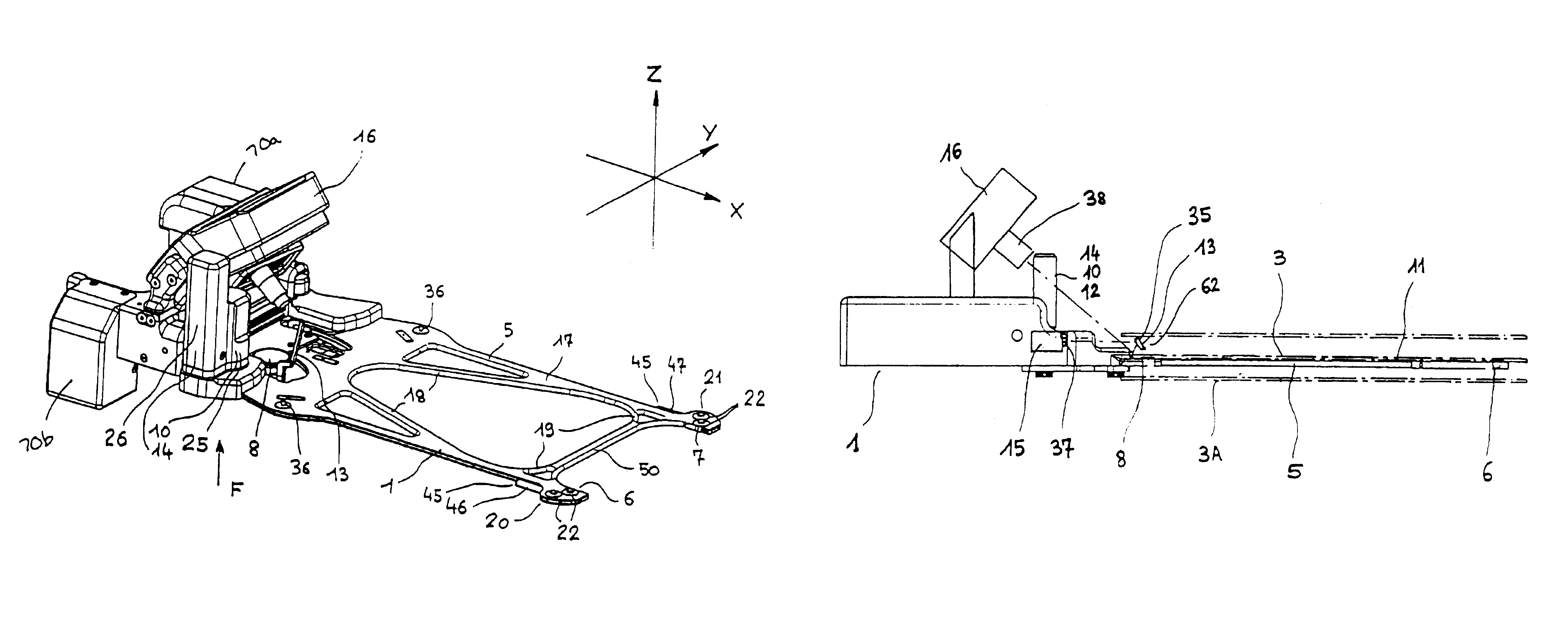
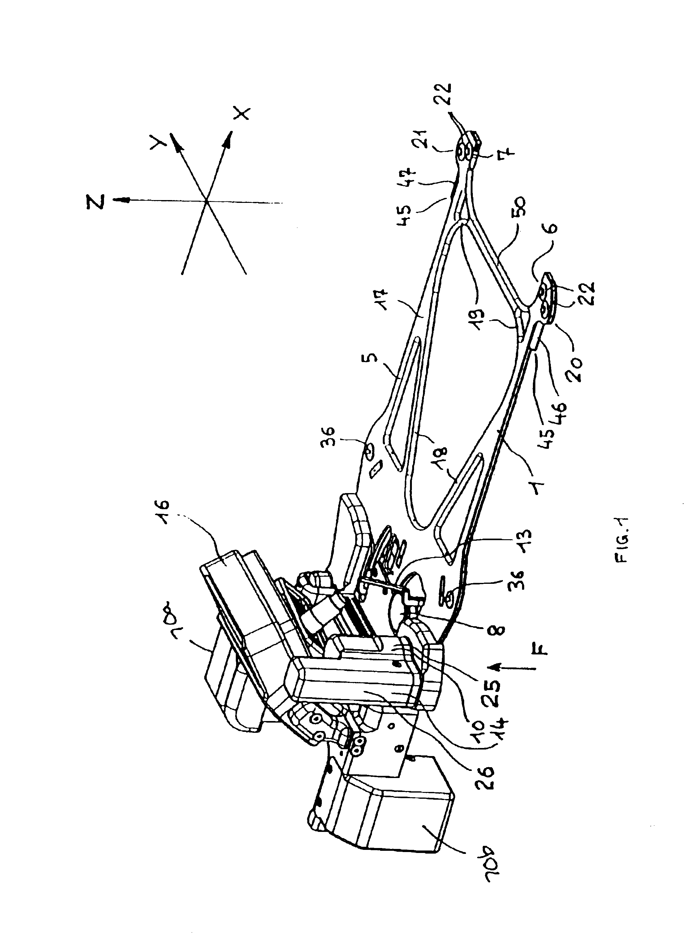
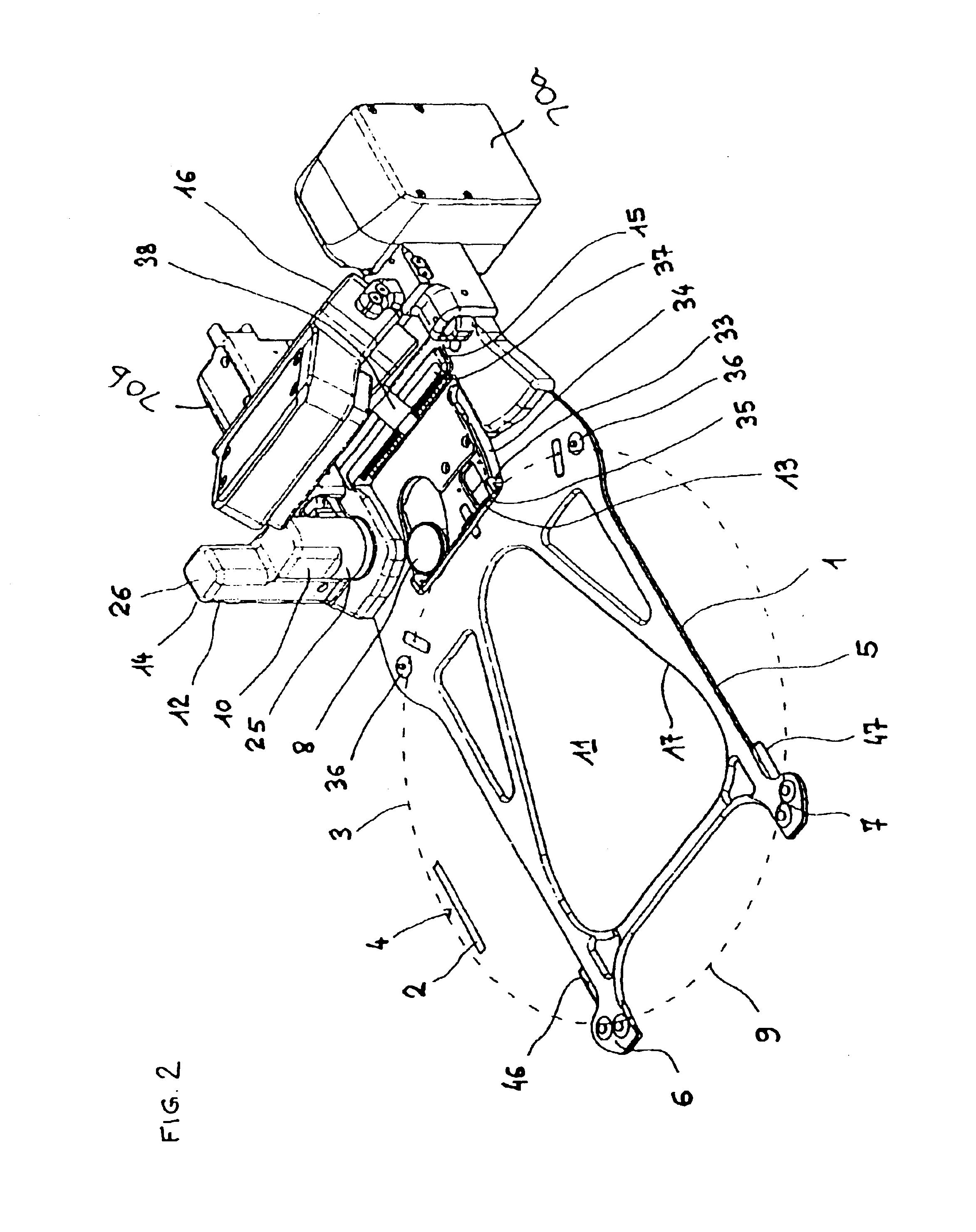
[0058]A presently preferred device 1 for identifying characters inscribed on a semiconductor wafer 3 containing at least one orientation mark 4 is shown in FIGS. 1 to 4. The preferred device 1 comprises a rigid grasping arm 5 in a specified plane 11. First and second rotary supports 6, 7 are each mounted on the grasping arm 5. Each rotary support 6 and 7 possesses one degree of freedom in rotation around its respective axis of symmetry. A third rotary support 8 is also mounted on the grasping arm 5. The third rotary support 8 also possesses one degree of rotational freedom around its axis of symmetry and one degree of freedom of movement in specified plane 11. The first 6, second 7 and third 8 rotary supports cooperate to support a semiconductor wafer 3 about its periphery, as shown in FIGS. 2 and 3.

[0059]The presently preferred device 1 also comprises a drive mechanism 10 which operates to displace third rotary support 8 in specified plane 11, a rotational drive mechanism 12 to rot...


PUM


Abstract

A device and process are provided for identifying characters inscribed on a semiconductor wafer containing an orientation mark. A semiconductor wafer having characters inscribed on a surface near its periphery is supported about its periphery between three rotary supports mounted on a grasping arm. An orientation mark on the periphery of the wafer is located adjacent the inscribed characters. At least one of the three rotary supports is rotatably driven to orient the wafer such that the orientation mark is placed in a determined position. An optical reflector is positioned in a spatial zone in proximity to and above the characters to be identified. The characters to be identified are illuminated by a light beam reflected by the optical reflector. The characters reflect the light, which may be observed by an optical imager, such as a camera. An optical recognition subsystem may then be used to identify the characters.

Description

BACKGROUND OF THE INVENTION[0001]1. Field of the Invention[0002]The present invention concerns the field of manufacturing electronic components, especially integrated circuits, on substrates or wafers made of semiconductor materials, like silicon, and especially concerns methods and devices for identifying characters inscribed on a semiconductor wafer containing at least one orientation mark.[0003]2. Description of the Art[0004]The prior art teaches several methods and devices for identifying characters inscribed on semiconductor wafers. In particular, a process for identifying characters engraved on substrates in the form of a wafer is known. This process consists of using a manipulator arm to hold a wafer horizontally, the wafer being one of a plurality of wafers arranged to be aligned one behind the other in respective grooves of a vertically arranged carrier, and removing the wafer from the carrier oriented at an angle by means of an orientation mark on its perimeter in the form...

Claims


Application Information

Patent Timeline
Patent Type & Authority Patents(United States)
IPC IPC(8): G06K7/10G06K9/20
CPCG06K7/10861Y10S414/141Y10S414/136H01L21/68
Inventor GAUDON, ALAINASTEGNO, PIERREEL JARJINI, MOHAMMED
Owner RECIF
Why Eureka
Try Eureka