

Image pickup apparatus
- Summary
- Abstract
- Description
- Claims
- Application Information
AI Technical Summary
Benefits of technology
Problems solved by technology
Method used
Image

Examples
first embodiment
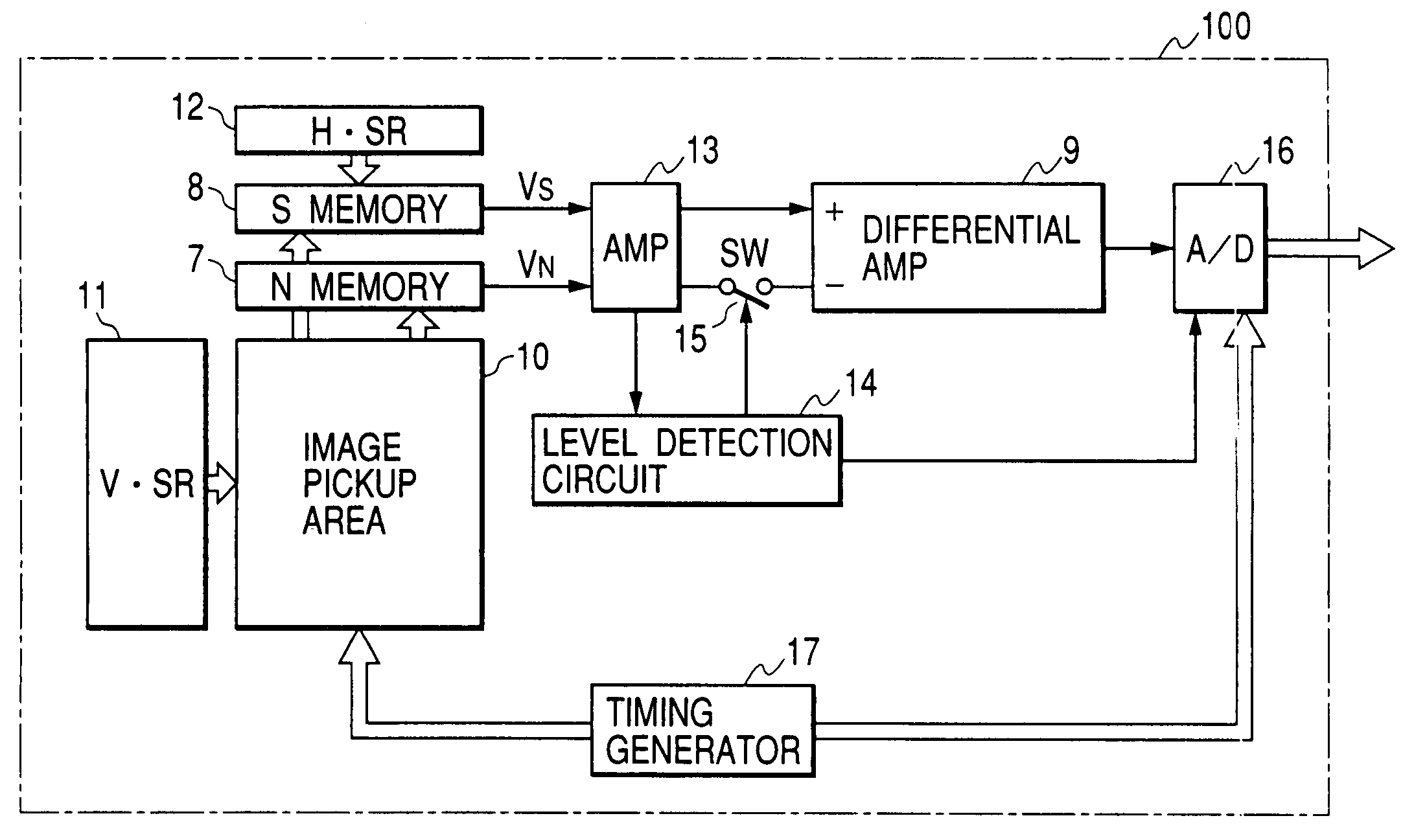
[0042]In the first embodiment, the level detection circuit detects whether the signal VS output from the S memory 8 is at signal level VA or more, thereby detecting saturation of the photodiode, or detects whether the signal VN output from the N memory 7 is at signal level VB or more, thereby detecting that the photo-leak noise signal v1 is a predetermined level or more.
[0043]When the level detection circuit 14 detects that the signal VS is at signal level VA or more, or the signal VN is at signal level VB or more, difference processing is not executed, thereby obtaining an image free from being darkened.
[0044]The first embodiment has exemplified the level detection circuit 14 as a detection means. However, the detection means suffices to detect image pickup conditions, and may be located not at the output stage of the amplifier 13 but, e.g., within the pixel.
[0045]The first embodiment has exemplified the switch 15 for stopping difference processing as a correction means. However, t...
second embodiment
[0052]The second embodiment has exemplified the level detection circuit 14 as a detection means. However, the detection means suffices to detect image pickup conditions, and may be located not at the output stage of the amplifier 13 but, e.g., within the pixel.
[0053]The second embodiment has exemplified as a correction means an arrangement of converting a signal read out from the memory into a signal of a predetermined level. However, the correction means suffices to perform correction of execution of difference processing in accordance with an output of the detection means, and may be located in, e.g., the image pickup area 10.
[0054]All the building elements of the solid-state image pickup apparatus 100 may be formed on a single semiconductor substrate by the CMOS process or the like. Alternatively, e.g., the A / D conversion circuit 16 and timing generator may be formed on different semiconductor substrates.
[0055]The pixels of the solid-state image pickup apparatus in the second emb...
third embodiment
[0059]the present invention will be described.
[0060]FIG. 9 is a block diagram showing an application of the solid-state image pickup apparatus in the first or second embodiment to a video camera serving as an image pickup system.
[0061]A photographing lens 201 comprises a focus lens 201A for adjusting the focus, a zoom lens 201B for performing zoom operation, and an imaging lens 201C.
[0062]An iris 202 is arranged after the photographing lens 201. A solid-state image pickup apparatus 100 described in the first or second embodiment photoelectrically converts an object image formed on the image pickup plane into an electrical image pickup signal. A process circuit 205 performs predetermined processing such as gamma correction, color separation, or blanking processing on a video signal output from the image pickup apparatus 100, and outputs a luminance signal Y and chrominance signals C. The chrominance signals C output from the process circuit 205 are subjected to white balance correcti...
PUM
 Abstract
Description
Claims
Application Information