Method for forming floating gate in flash memory device

a technology of flash memory and floating gate, which is applied in the direction of semiconductor devices, electrical devices, transistors, etc., can solve the problem that buffer oxide films cannot be uniformly maintained on the whole surface of wafers, and achieve the effect of preventing the thickness of buffer oxide films

Inactive Publication Date: 2005-11-15
STMICROELECTRONICS SRL +1
View PDF4 Cites 11 Cited by
  • Summary
  • Abstract
  • Description
  • Claims
  • Application Information

AI Technical Summary

Benefits of technology

[0005]Accordingly, a method for a floating gate in a flash memory device is disclosed which is capable of preventing a thickness of a buffer oxide film from being increased due to a first polysilicon film in a subsequent wall oxidation process according to a deposition of the buffer oxide film and which is capable of minimizing an attack of the first polysilicon film during a pad nitride film strip process.

Problems solved by technology

Accordingly, there is a problem that the buffer oxide film cannot uniformly remain over a whole surface of a wafer.

Method used


Image

  • Method for forming floating gate in flash memory device
  • Method for forming floating gate in flash memory device
  • Method for forming floating gate in flash memory device

Examples


Embodiment Construction

[0016]Now, preferred embodiments will be described in detail with reference to the appended drawings. However, this disclosure is not limited to the embodiments disclosed in the following description, but various changes and modifications will be apparent to those skilled in the art.

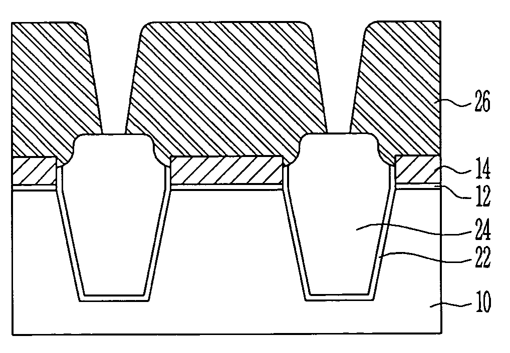
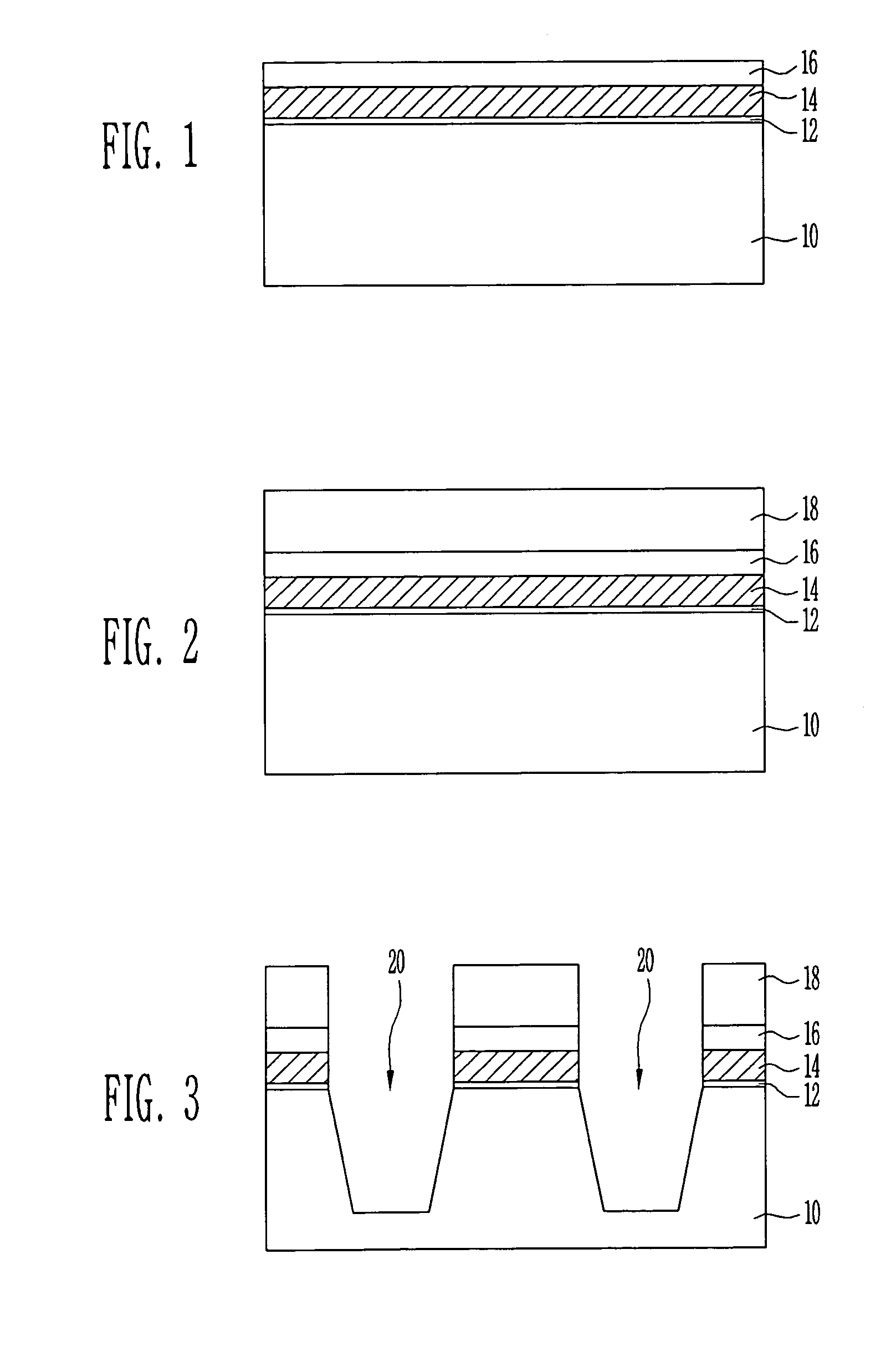
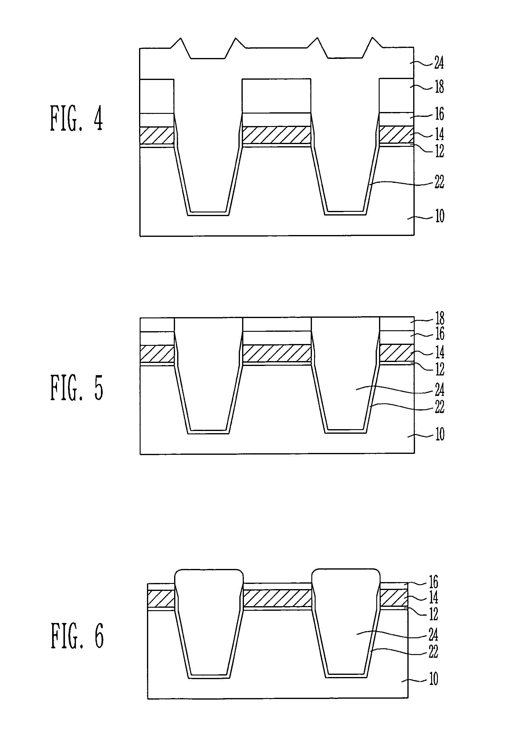
[0017]FIGS. 1 to 9 are cross-sectional views illustrating a method of forming a floating gate of a flash memory device according to one embodiment.

[0018]Referring to FIG. 1, a semiconductor substrate 10 cleaned using a pre-treatment cleaning process is provided. In case of performing the pre-treatment cleaning process, a diluted HF (DHF) is used and then an SC-1 (NH4OH / H2O2 / H2O) is used, or a buffer oxide etchant (BOE) is used and then the SC-1 is used. An ion implantation process for forming wells (not shown) and an ion implantation process for controlling a threshold voltage are carried out after the cleaning process is carried out. At that time, the ion implantation processes are carried out using a s...


PUM


Abstract

The present invention is provided to form a floating gate of a flash memory device capable of restricting a thickness of a buffer oxide film to a thickness less than 50 Å to minimize increment in a thickness due to a wall oxidation process in the case of depositing the buffer oxide film prior to depositing the first polysilicon film and the pad nitride film, and reducing a thickness of the first polysilicon film with an HF dip time minimized in a pre-treatment cleaning process prior to depositing the second polysilicon film, and protecting the first polysilicon film from being attacked in a pad nitride film strip process, by removing at least 50% of the buffer oxide film in the pad nitride film strip process.

Description

BACKGROUND[0001]1. Technical Field[0002]A method for forming a floating gate in a flash memory device is disclosed capable of preventing a thickness of a buffer oxide film from being increased due to a first polysilicon film in a subsequent wall oxidation process, and which is capable of minimizing an attack of the first polysilicon film during a pad nitride film strip process.[0003]2. Discussion of Related Art[0004]In recent, a self-aligned shallow trench isolation (SA-STI) process has been used as a device isolation process in realizing a highly integrated NAND flash memory device. Accordingly, a floating gate is divided into a first polysilicon film and a second polysilicon film to form a stack structure. At that time, a buffer oxide film is deposited with a suitable thickness prior to depositing the first polysilicon film and a pad nitride film for the purpose of relieving a stress between the pad nitride film and the first polysilicon film. This buffer oxide film is used as a b...

Claims


Application Information

Patent Timeline
Patent Type & Authority Patents(United States)
IPC IPC(8): H01L21/70H01L27/115H01L21/8247H01L29/788H01L29/792
CPCH01L27/115H01L27/11521H10B69/00H10B41/30
Inventor DONG, CHA DEOKHAN, IL KEOUN
Owner STMICROELECTRONICS SRL
Why Eureka
Try Eureka