Substrate processing apparatus and method of manufacturing semiconductor device

a processing apparatus and semiconductor technology, applied in the direction of individual semiconductor device testing, semiconductor/solid-state device testing/measurement, instruments, etc., can solve the problems of non-uniform plasma generation, non-uniform film thickness of process-target substrate, and ineffective means for checking the shape variation of discharge electrodes in the conventional ar

Active Publication Date: 2012-01-10
KOKUSA ELECTRIC CO LTD
View PDF5 Cites 15 Cited by
  • Summary
  • Abstract
  • Description
  • Claims
  • Application Information

AI Technical Summary

Benefits of technology

[0008]An object of the present invention is to provide a substrate processing apparatus and a method of manufacturing a semiconductor device, in which shape variations of discharge electrodes can be early detected so as to prevent a film having anon-uniform thickness from being formed on a substrate.

Problems solved by technology

In this case, plasma is non-uniformly generated, and thus the film thickness of a process-target substrate becomes non-uniform.
However, there no effective means for checking shape variations of the discharge electrodes in the conventional art, and in many cases, shape variations of the discharge electrodes are detected only after the film thickness of the process-target substrate has become non-uniform.

Method used


Image

  • Substrate processing apparatus and method of manufacturing semiconductor device
  • Substrate processing apparatus and method of manufacturing semiconductor device
  • Substrate processing apparatus and method of manufacturing semiconductor device

Examples


Embodiment Construction

[0021]According to preferred embodiments of the present invention, a substrate processing apparatus is configured as an example of a semiconductor manufacturing apparatus used to perform a processing process in a method of manufacturing a semiconductor device such as an integrated circuit (IC) device.

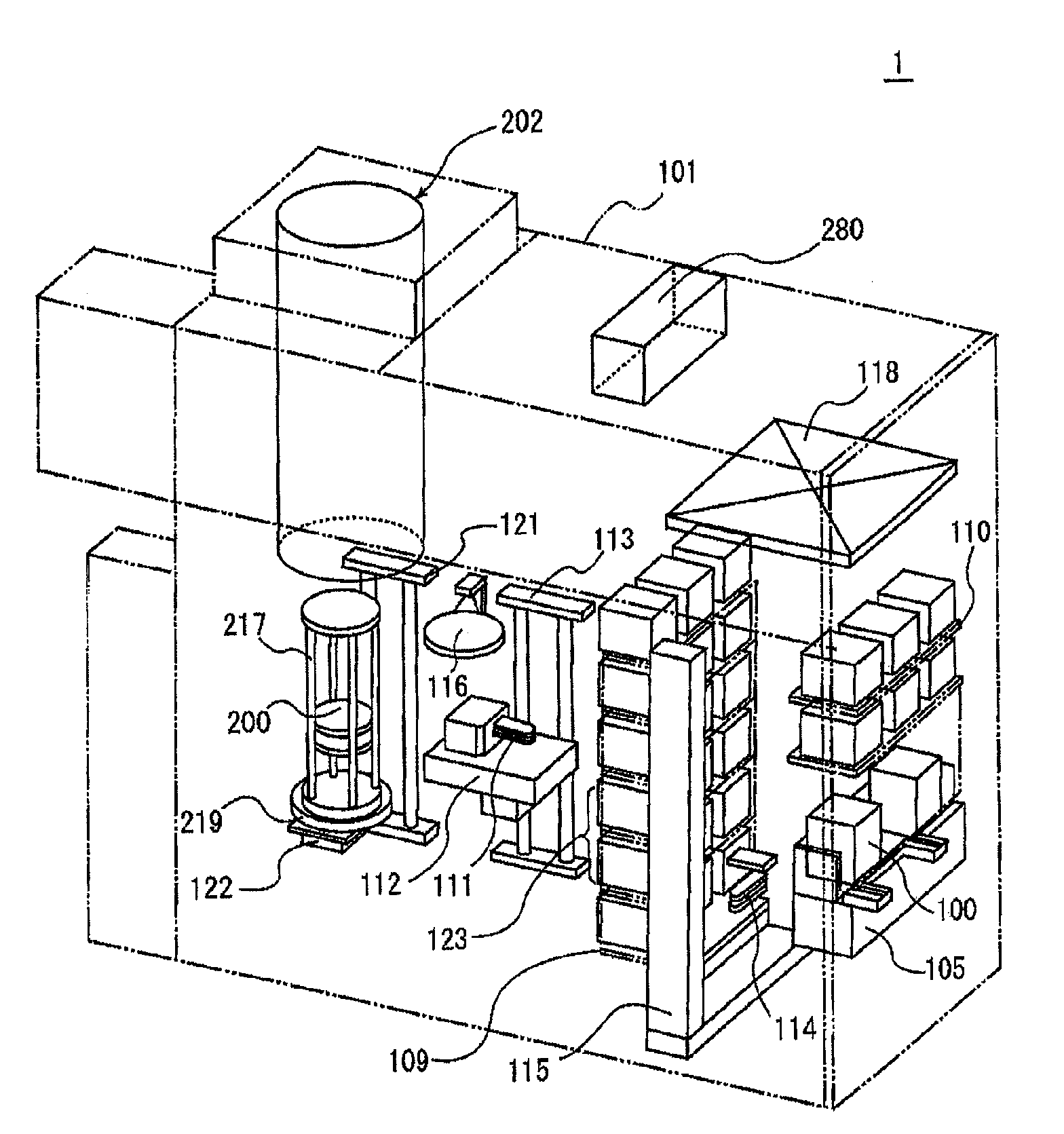
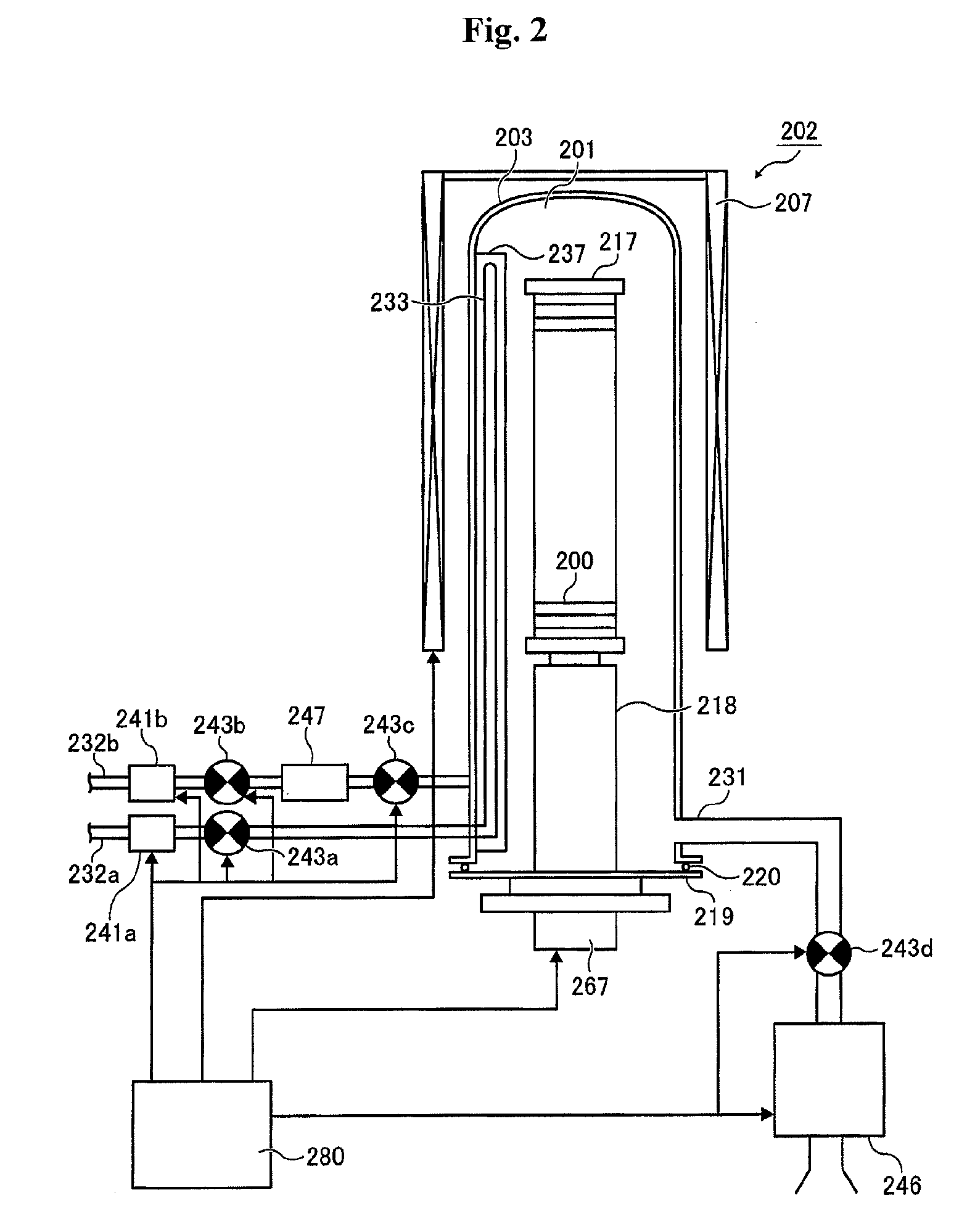
[0022]Furthermore, in the following description, as a substrate processing apparatus, a vertical apparatus configured to perform a process such as oxidation, diffusion or chemical vapor deposition (CVD) on a substrate will be explained (hereinafter, the vertical apparatus will also be simply referred to as a processing apparatus). FIG. 1 is a perspective view illustrating a processing apparatus according to the present invention.

[0023]As shown in FIG. 1, in a processing apparatus 1 of the current embodiment, cassettes 100 are used as wafer carriers for accommodating wafers (substrates) 200 made of a material such as silicon, and the processing apparatus 1 includes a case 101. At the ins...


PUM

PropertyMeasurementUnit
temperatureaaaaaaaaaa
pressureaaaaaaaaaa
pressureaaaaaaaaaa

Abstract

Provided are a substrate processing apparatus and a method of manufacturing a semiconductor device, in which shape variations of discharge electrodes can be early detected so as to prevent a film having a non-uniform thickness from being formed on a substrate. The substrate processing apparatus includes a process chamber configured to stack a plurality of substrates therein, a gas supply unit configured to supply gas to an inside of the process chamber, at least one pair of electrodes installed in the process chamber and configured to receive high-frequency power to generate plasma that excites the gas supplied to the inside of the process chamber, and a monitoring system configured to monitor a shape variation of the electrodes.

Description

CROSS-REFERENCE TO RELATED PATENT APPLICATION[0001]This U.S. non-provisional patent application claims priority under 35 U.S.C. §119 of Japanese Patent Application No. 2008-300961, filed on Nov. 26, 2008, in the Japanese Patent Office, the entire contents of which are hereby incorporated by reference.BACKGROUND OF THE INVENTION[0002]1. Field of the Invention[0003]The present invention relates to a substrate processing apparatus configured to perform an etching process or a film forming process on the surface of a substrate such as a semiconductor wafer, and a method of manufacturing a semiconductor device.[0004]2. Description of the Prior Art[0005]As an example of substrate processing apparatuses, a semiconductor manufacturing apparatus is known, and as an example of semiconductor manufacturing apparatuses, a vertical diffusion chemical vapor deposition (CVD) apparatus is known. Such a vertical diffusion CVD apparatus includes a narrow and long vertical buffer chamber at a position ...

Claims


Application Information

Patent Timeline
Patent Type & Authority Patents(United States)
IPC IPC(8): H01L21/66H01L21/67
CPCC23C16/45542C23C16/45546C23C16/509C23C16/52H01L21/3185H01L21/67253H01L21/02211H01L21/0228H01L21/0217H01L21/02274
Inventor ISHIMARU, NOBUO
Owner KOKUSA ELECTRIC CO LTD
Why Eureka
Try Eureka