Tunneling diode magnetic junction memory

a magnetic junction memory and diode technology, applied in the field of memory devices, can solve the problems of inaccurate or erroneous reading of the contents of the memory cell, reduce yield, add additional expense, etc., and achieve the effect of prolonging the storage life of the memory cell

Active Publication Date: 2005-11-15
MACRONIX INT CO LTD
View PDF7 Cites 29 Cited by
  • Summary
  • Abstract
  • Description
  • Claims
  • Application Information

AI Technical Summary

Benefits of technology

[0010]The present invention discloses a magnetic memory structure that eliminates the need for a separate semiconductor diode. The present invention further discloses an innovative method of reading the contents of a memory cell in order to extend the storage life of the memory cell.
[0011]In accordance with one aspect of the present invention, a magnetic memory cell comprises a first ferromagnetic layer and a second ferromagnetic layer. An insulating layer is disposed between the first and second ferromagnetic layers. The insulating layer forms a diode that prevents leakage currents. Several of the memory cells are formed into an array of memory cells. The array of memory cells is interconnected by column conductor lines and row conductor lines that are oriented perpendicularly to each other.
[0013]In accordance with another aspect of the present invention, a memory cell comprises a fixed magnetic layer that has a magnetic moment that is fixed in a pre-determined direction. A free magnetic layer has a magnetic moment that is free to rotate under the influence of an applied magnetic field. An insulating layer is disposed between the fixed and free magnetic layers. A tunneling diode is formed by the insulating layer in combination with the fixed and free magnetic layers. The tunneling diode allows a current between the free magnetic layer when selected and the fixed magnetic layer when selected and prevents leakage current between the fixed magnetic and free magnetic layers when not selected. Several of the memory cells are formed into a memory cell array. The memory cells are interconnected by column conductor lines and row conductor lines. A memory cell is located at the junction of each column line and conductor line. The column lines are connected to the free magnetic layers and the row lines are connected to the fixed magnetic layers.
[0014]In accordance with another aspect of the present invention, a method of reading an array of memory cells comprises providing several column lines and row lines that are connected across the array of memory cells. A column line and a row line are selected during a first read cycle such that a first current flows from the column line through a first memory cell to the row line. The current flows from the row line to the column line during a second read cycle. The current flow is thus reversed during the second read cycle of the first memory cell such that the storage life of the memory cell is extended. The direction of current flow through the first memory cell is reversed for each subsequent read cycle. The number of read cycles is recorded for each memory cell in the array.

Problems solved by technology

Such leakage currents can lead to inaccurate or erroneous readings of the contents of the memory cell.
Unfortunately, the semiconductor diode can be difficult to fabricate on the memory cell, can add additional expense and can lead to lower yields.
Another problem exists with the storage times of magnetic memory cells.

Method used


Image

  • Tunneling diode magnetic junction memory
  • Tunneling diode magnetic junction memory
  • Tunneling diode magnetic junction memory

Examples


Embodiment Construction

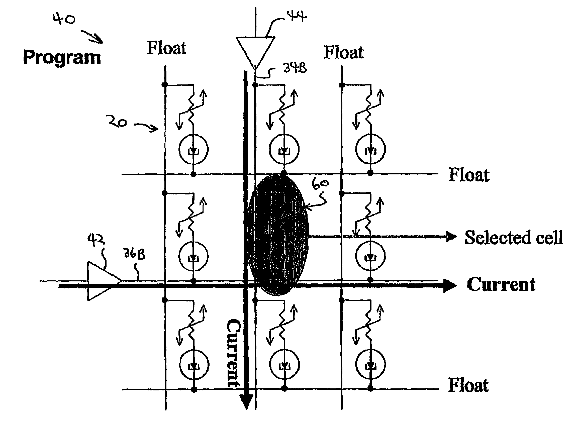
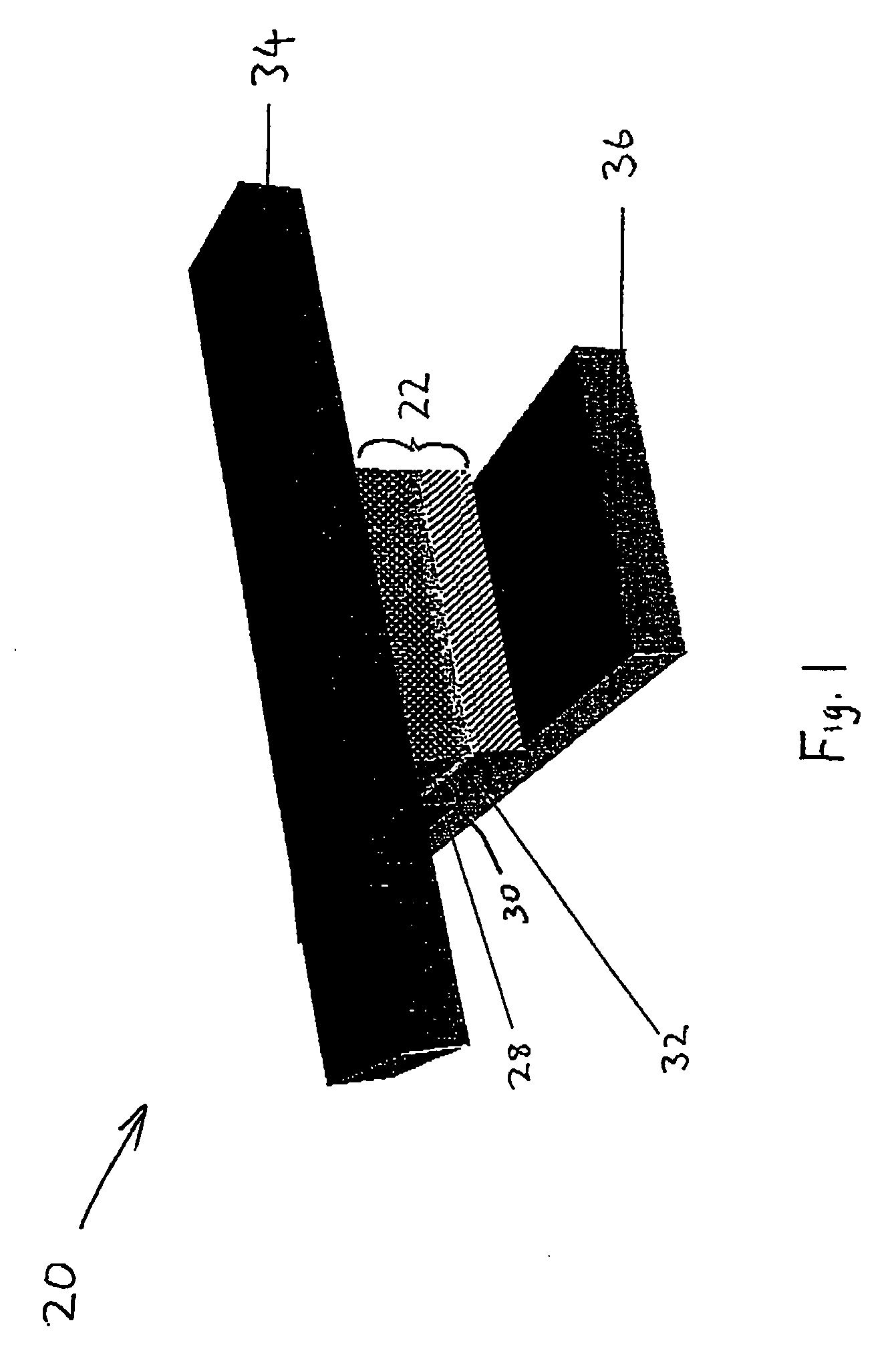
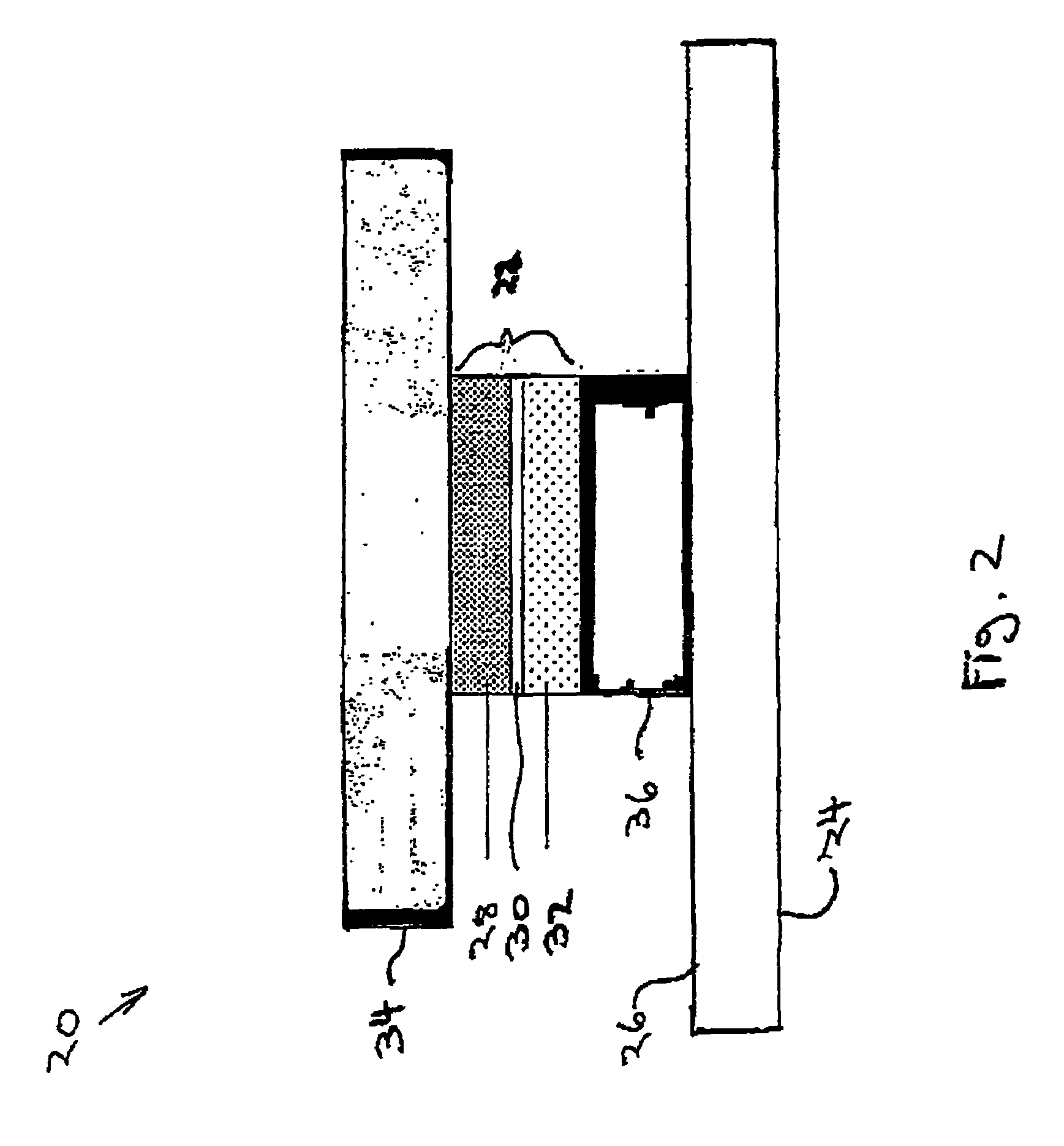
[0026]Reference will now be made in detail to the presently preferred embodiments of the invention, examples of which are illustrated in the accompanying drawings. Wherever possible the same or similar reference numbers are used in the drawings and the description to refer to the same or like parts. It should be noted that the drawings are in simplified form and are not to precise scale. In reference to the disclosure herein for purposes of convenience and clarity only, directional terms, such as top, bottom, left, right, up, down, over, above, below, beneath, rear, front, vertical, horizontal, length, width, and height are used with respect to the accompanying drawings. Such directional terms should not be construed to limit the scope of the invention in any manner.

[0027]Although the disclosure herein refers to certain illustrated embodiments, it is to be understood that these embodiments are presented by way of example and not by way of limitation. The intent of the following deta...


PUM


Abstract

A tunneling diode magnetic junction memory that eliminates the need for a separate semiconductor diode is disclosed. The diode is formed by an insulating layer that is located between a free magnetic layer and a pinned magnetic layer. The present invention further discloses a method of reading the contents of a memory cell in a bi-directional manner in order to extend a storage life of the memory cell.

Description

BACKGROUND OF THE INVENTION[0001]1. Field of the Invention[0002]The present invention relates generally to memory devices and, more particularly, to a non-volatile magnetic memory devices.[0003]2. Description of Related Art[0004]Integrated circuits, typically in the form of microprocessors, microcontrollers, or other logic circuits, are used to control the functions of many modern electronic devices. For example, integrated circuits are used to control the functions of computers, telephones, and many other consumer electronics. It is generally necessary for the integrated circuits to retrieve (read) and store (write) data as they perform their functions. The data may be in the form of instructions for the integrated circuits (e.g., a program), data necessary for the execution of a program, or data generated during the execution of the program. It is preferable to store the data in memory devices which are easily accessible by the integrated circuits.[0005]Many different types of mem...

Claims


Application Information

Patent Timeline
Patent Type & Authority Patents(United States)
IPC IPC(8): G11C11/15G11C11/02G11C11/14
CPCG11C11/16H01L43/08H10N50/10
Inventor LUNG, HSIANG-LANLIU, RUICHEN
Owner MACRONIX INT CO LTD
Why Eureka
Try Eureka