
Eureka
For R&D, Eureka makes reading and utilizing patents & technical documents easy.
Eureka AIR
Designed for self-driven R&D workflows. Generate viable solutions, solve complex R&D challenges, empower your innovation with AI.

Eureka Materials
Designed for material experts only. Revolutionize your material R&D, from search, analyze, to developing new materials.

TechResearch
Generate reliable direction feasibility study reports for your R&D in just a few steps.

TechSeek
Discover and master advanced knowledge NOW. Basics, ideas, possibilities, all at once.

TechMind
As an expert in R&D Theories, TechMind can generates customized viable solutions instantly.

TechRisk
Analyze your overall solution with one click, know your potential R&D risks in advance.

TechMonitor
Get weekly tech updates, stay abreast of the latest tech innovations and key insights.
Semiconductor device and method of manufacturing the same
- Summary
- Abstract
- Description
- Claims
- Application Information
AI Technical Summary
Benefits of technology
Problems solved by technology
Method used
Image

Examples
embodiment 1
(Embodiment 1)
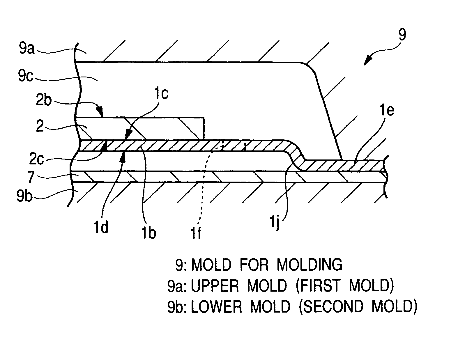
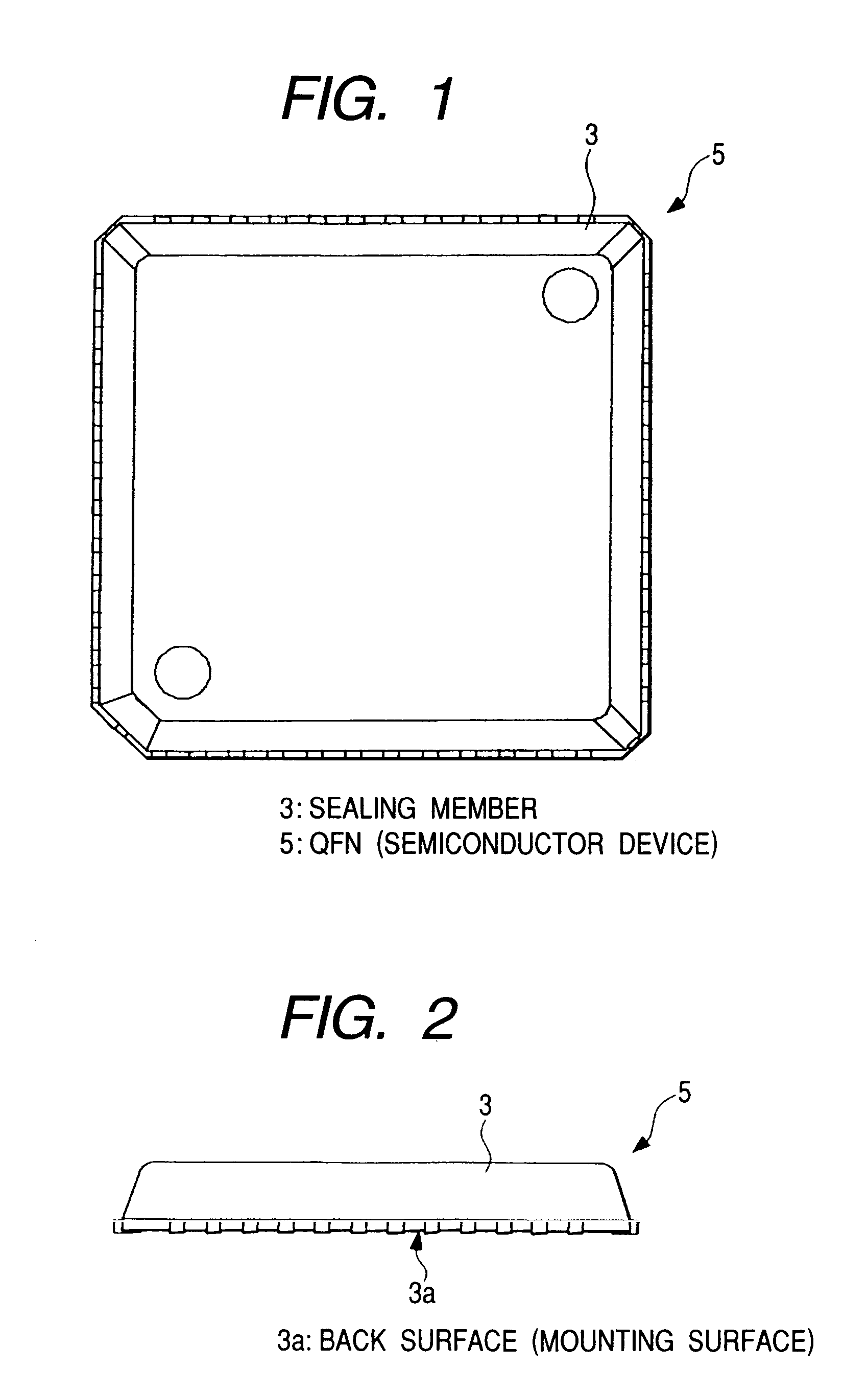
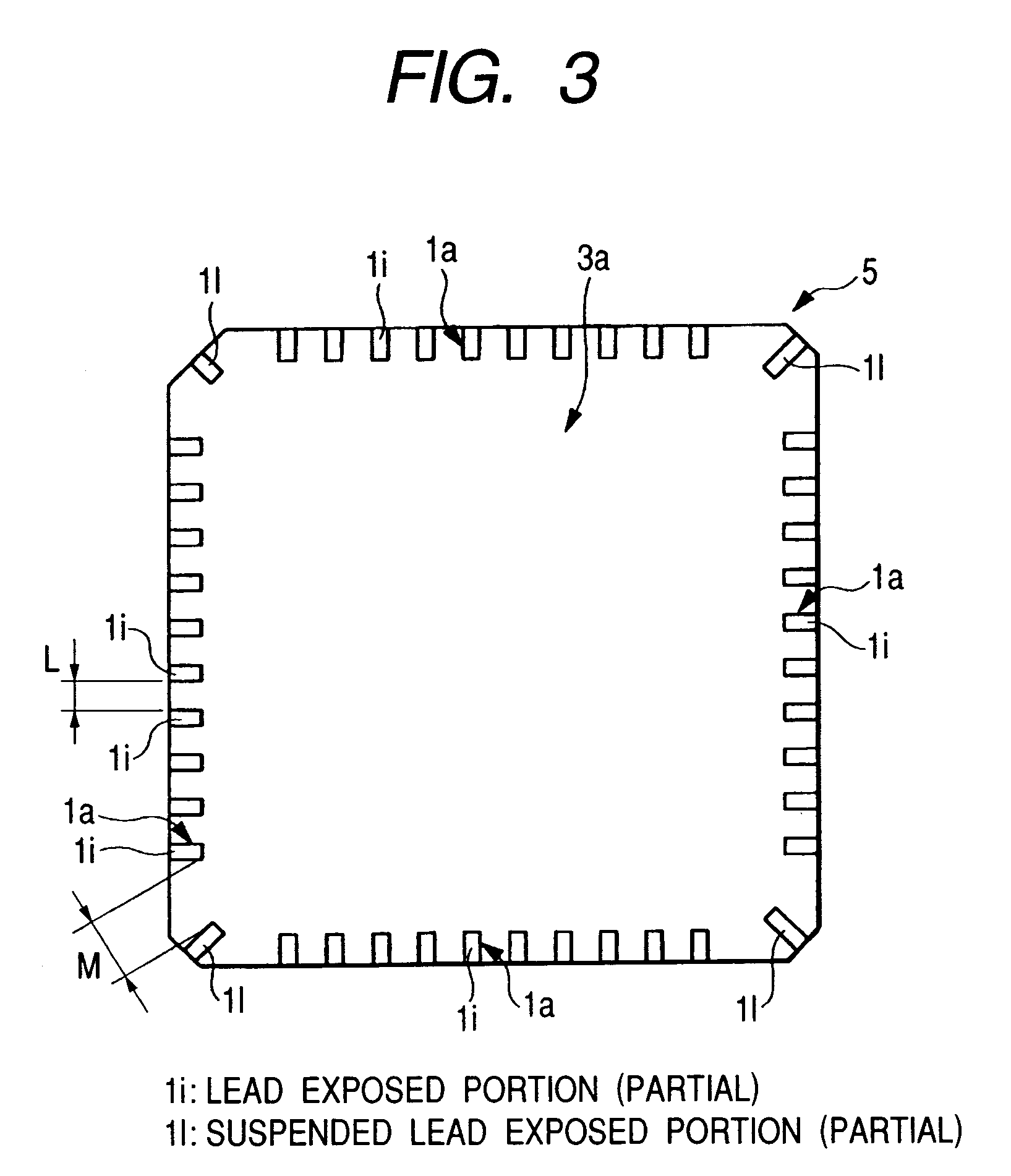
[0053]FIG. 1 is a plan view showing one example of a structure of a semiconductor device (QFN) of the embodiment 1 of the present invention. FIG. 2 is a side view showing one example of the structure of the QFN shown in FIG. 1. FIG. 3 is a bottom view showing one example of the structure of the QFN shown in FIG. 1. FIG. 4 is a cross-sectional view showing one example of the structure of a cross-section of the QFN shown in FIG. 1 taken along a line A—A shown in FIG. 8. FIG. 5 is a cross-sectional view showing one example of the structure of a cross-section of the QFN shown in FIG. 1 taken along a line B—B shown in FIG. 8. FIG. 6 is a circuit block diagram showing one example of the constitution of a circuit of a logic chip incorporated into the QFN shown in FIG. 1. FIG. 7 is a partial plan view showing one example of the structure of a lead frame served for assembling of the QFN shown in FIG. 1. FIG. 8 is a partial plan view showing one example of the structure of the Q...
embodiment 2
(Embodiment 2)
[0109]FIG. 15 is a partial cross-sectional view showing one example of a cross-sectional structure of a semiconductor device (QFN) of the embodiment 2 of the present invention by cutting the semiconductor device at a C portion shown in FIG. 16, FIG. 16 is a partial plan view showing one example of the structure of the QFN shown in FIG. 15 after wire bonding in assembling of the QFN, FIG. 17 is a bottom view showing one example of the structure of the QFN shown in FIG. 15, FIG. 18 is a partial plan view showing one example of an arrangement of terminals of a mounting substrate on which the QFN shown in FIG. 15 are mounted, FIG. 19 is a partial cross-sectional view showing one example of a structure for mounting the QFN shown in FIG. 15 on a mounting substrate by cutting the mounting structure at a lead position and FIG. 20 is a partial cross-sectional view showing one example of a structure for mounting the QFN shown in FIG. 15 on a mounting substrate by cutting the mou...
embodiment 3
(Embodiment 3)
[0121]FIG. 21 is a partial cross-sectional view showing one example of a cross-sectional structure of a semiconductor device (QFN) of the embodiment 3 of the present invention by cutting the semiconductor device at a D portion shown in FIG. 22, FIG. 22 is a partial plan view showing one example of the structure after wire bonding in assembling of the QFN shown in FIG. 21, FIG. 23 is an enlarged partial cross-sectional view showing one example of a double-sized pad of a semiconductor chip shown in FIG. 22, FIG. 24 is a bottom view showing one example of the structure of the QFN shown in FIG. 21, FIG. 25 is a partial plan view showing one example of a terminal arrangement of a mounting substrate on which the QFN shown in FIG. 21 is mounted, FIG. 26 is a partial cross-sectional view showing one example of a structure for mounting the QFN shown in FIG. 21 to the mounting substrate by cutting the mounting structure at a lead position and FIG. 27 is a partial cross-sectional...
PUM
 Abstract
Description
Claims
Application Information
 - R&D Engineer
- R&D Manager
- IP Professional
- Industry Leading Data Capabilities
- Powerful AI technology
- Patent DNA Extraction
Browse by: Latest US Patents, China's latest patents, Technical Efficacy Thesaurus, Application Domain, Technology Topic, Popular Technical Reports.
© 2024 PatSnap. All rights reserved.Legal|Privacy policy|Modern Slavery Act Transparency Statement|Sitemap|About US| Contact US: help@patsnap.com