Eureka AIR delivers breakthrough ideas for toughest innovation challenges, trusted by R&D personnel around the world.

Method of forming dual gate insulator layers for CMOS applications

Inactive Publication Date: 2005-11-22
TAIWAN SEMICON MFG CO LTD
View PDF16 Cites 7 Cited by
  • Summary
  • Abstract
  • Description
  • Claims
  • Application Information

AI Technical Summary

Benefits of technology

[0007]It is another object of this invention to apply a HF type pre-clean procedure prior to formation of each gate insulator layer, without degrading the thickness of the exposed first gate insulator layer during the application of a second HF type pre-clean procedure, applied prior to second gate insulator formation.

Problems solved by technology

If the pre-clean procedure is omitted the inclusion of the native oxide will degrade the quality of the regrown, thin insulator layer.
However if the pre-clean procedure is employed the exposed thicker insulator layer will be thinned, perhaps to a point deleteriously influencing the performance or reliability of the I / O device featuring the thicker gate insulator component.

Method used


Image

  • Method of forming dual gate insulator layers for CMOS applications
  • Method of forming dual gate insulator layers for CMOS applications
  • Method of forming dual gate insulator layers for CMOS applications

Examples


Embodiment Construction

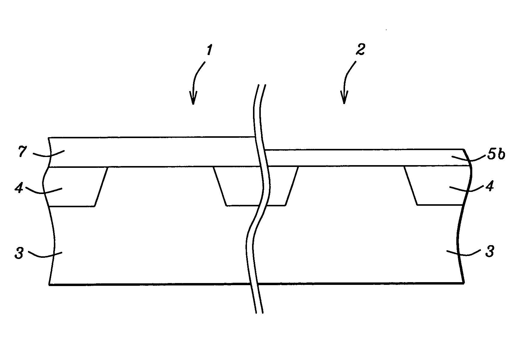
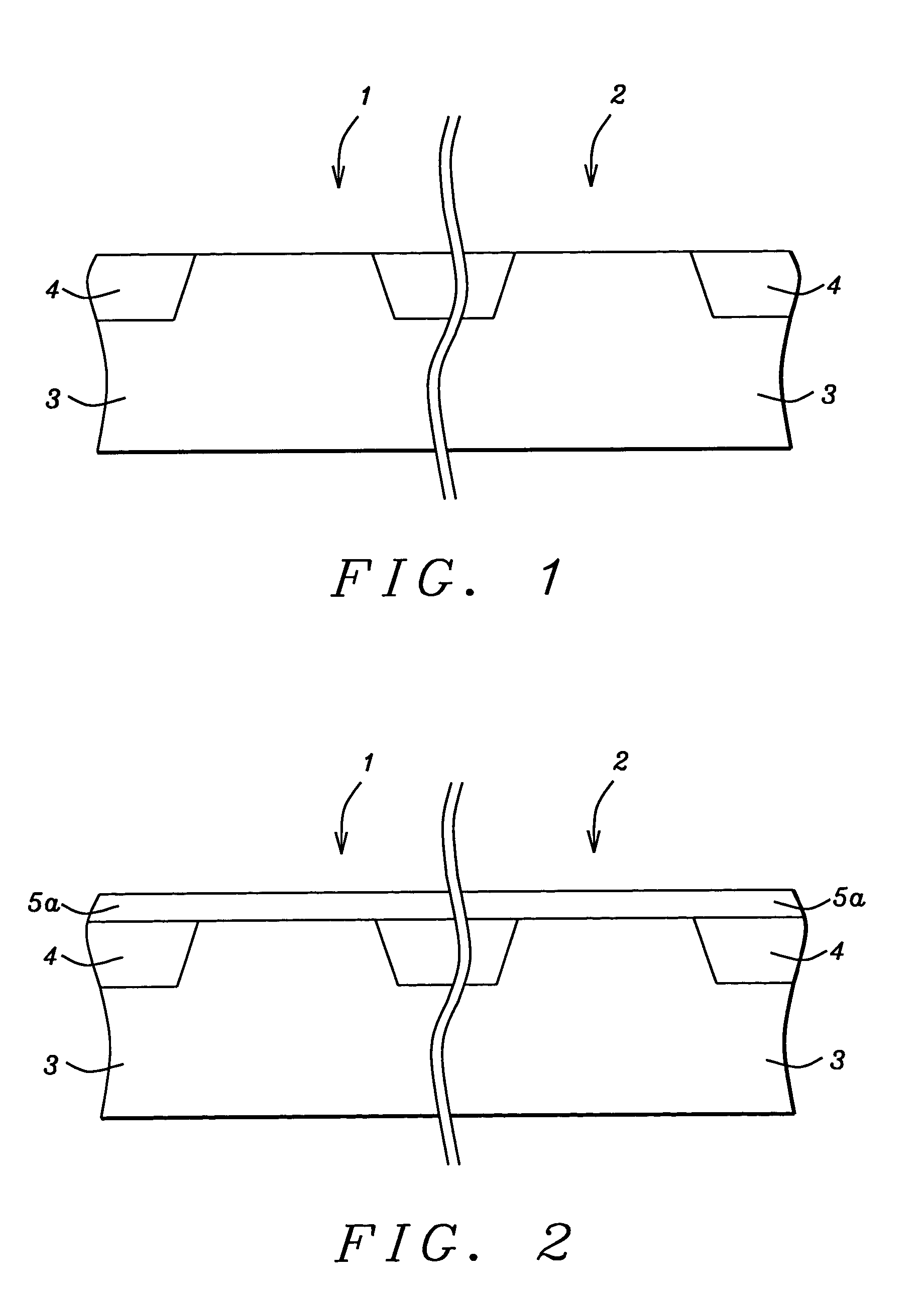
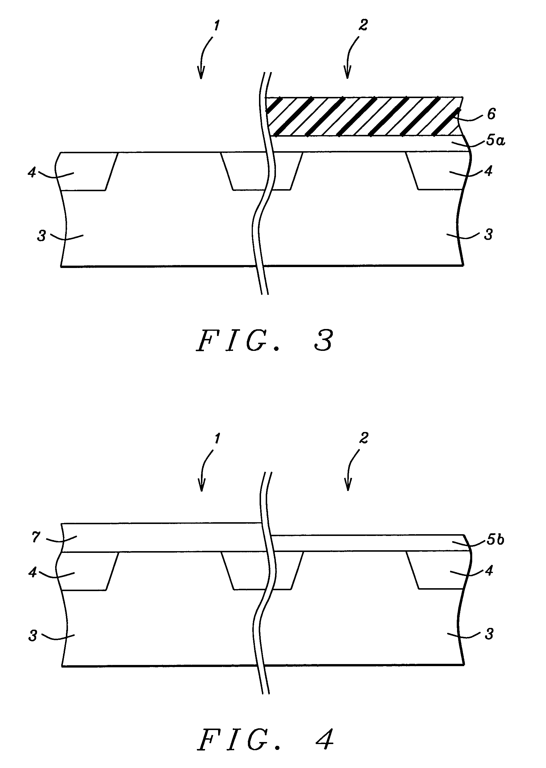
[0012]The method of forming dual gate insulator layers, each comprised of a specific thickness, featuring the use of HF type pre-cleans applied prior to formation of each of the gate insulator layers, will now be described in detail. Semiconductor substrate 3, comprised of P type, single crystalline silicon, featuring a crystallographic orientation, is used and schematically shown in FIG. 1. Region 1, of semiconductor substrate 3, will be reserved for accommodation of I / O type, CMOS devices, wherein the I / O type devices will subsequently operate at higher voltages than counterpart core type CMOS devices, to subsequently by formed in region 2, of semiconductor substrate 3. Shallow trench isolation (STI), regions 4, comprised of silicon oxide filled shallow trench shapes, are formed for isolation between the I / O and core devices, as well as to isolate and define specific active device regions of each type CMOS device. This is schematically shown in FIG. 1.

[0013]Prior to formation of ...


PUM


Abstract

A method of forming dual gate insulator layers, each with a specific insulator thickness, featuring a HF type pre-clean procedure performed prior to formation of each of the gate insulator layers, has been developed. After a first HF type pre-clean procedure a silicon nitride layer is deposited on the native oxide free, semiconductor substrate followed by selective removal of silicon nitride layer from a second portion of the semiconductor substrate. After a second HF type pre-clean procedure a silicon dioxide gate insulator layer is formed on the second portion of the native oxide free, semiconductor substrate, with the silicon dioxide gate insulator layer comprised with a different thickness than the silicon nitride gate insulator layer, located on a first portion of the semiconductor substrate. The procedure used to form the silicon dioxide gate insulator layer also removes bulk traps in the silicon nitride gate insulator layer.

Description

BACKGROUND OF THE INVENTION[0001](1) Field of the Invention[0002]The present invention relates to method used to fabricate semiconductor devices, and more specifically to a method used to form dual gate dielectric layers for specific applications of complimentary metal oxide semiconductor (CMOS), devices, wherein one of the gate dielectric layers is a silicon nitride layer.[0003](2) Description of Prior Art[0004]Advanced CMOS designs are formed for multiple applications with each application requiring a specific CMOS type device, in turn necessitating the fabrication of different type CMOS devices on the same semiconductor chip. For example CMOS devices such as a device used for input / output (I / O) applications require thicker gate insulator layers for I / O operation than counterpart CMOS devices used for core memory applications, which in turn are used at lower operating voltages thus requiring thinner gate insulator layers. Therefore to satisfy the requirements of the different CMOS...

Claims


Application Information

Patent Timeline
IPC IPC(8): H01L21/70H01L21/8238
CPCH01L21/823857Y10S438/981
Inventor CHEN, CHI-CHUNLEE, TZU-LIANGCHEN, SHIH-CHANG
Owner TAIWAN SEMICON MFG CO LTD
Why Eureka
Eureka Blog
Learn More