Dual ramp rate dielectric breakdown testing methodology

a dielectric breakdown and ramp rate technology, applied in the direction of individual semiconductor device testing, semiconductor/solid-state device testing/measurement, instruments, etc., can solve the problem of reducing the yield of the device, the dielectric strength of new insulators no longer has the density of pure dense amorphous silicon oxide, and the inability to test a sufficient number of duts to obtain good enough statistics, etc., to achieve the effect of improving the screening of microelectronic devices

Active Publication Date: 2005-11-22
TEXAS INSTR INC
View PDF4 Cites 27 Cited by
  • Summary
  • Abstract
  • Description
  • Claims
  • Application Information

AI Technical Summary

Problems solved by technology

However, these new insulators no longer have the dielectric-strength of pure dense amorphous silicon oxides; their lower density and the presence of weaker bonds (such as Si—C bonds) introduce charge traps, and can potentially host mobile ions, that aid early breakdown events under electrical stress.
Since TDDB tests are slow, one cannot test sufficient number of DUTs to obtain good enough statistics.
Thus, in many instances, reliable devices are discarded as scrape although their dielectrics had no defects, thereby reducing device yield.
This is highly undesirable given the cost of manufacture and the loss of potential profit.

Method used


Image

  • Dual ramp rate dielectric breakdown testing methodology
  • Dual ramp rate dielectric breakdown testing methodology
  • Dual ramp rate dielectric breakdown testing methodology

Examples


Embodiment Construction

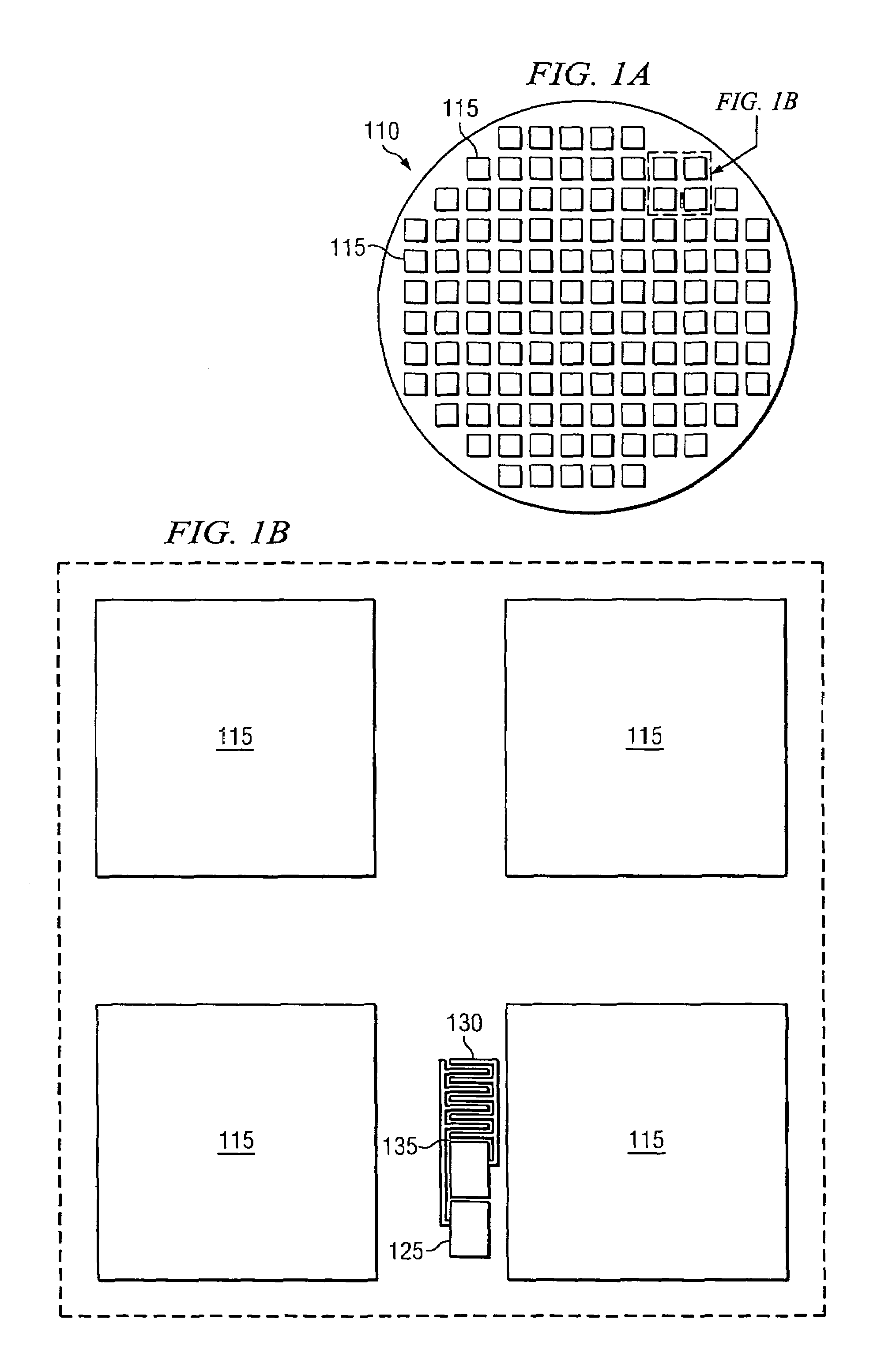
[0023]Turning initially to FIG. 1A there is illustrated an overhead view of a wafer 110, such as a microelectronics wafer or a semiconductor wafer, having integrated circuit die 115 located, thereon, as shown in FIG. 1A and FIG. 1B which is a magnified view of a delineated portion of FIG. 1A, that contain conventional integrated circuits (not shown). Associated with at least one die 115, or group of die, is a test device 125, which is schematically shown and is enlarged for illustrative purposes only. The number of test devices 125 may vary, and each die 115 may have a test device 125 associated with it, or a group of die may have one test device 125 associated therewith, which is the case shown in FIG. 1B. A group of test devices 125 forms a test sample, and in advantageous embodiments, it is desirable to have the test sample as large and mixed as practical to get a good statistical sampling across the wafer 110. It should also be noted that in some embodiments, especially during d...


PUM


Abstract

The present invention provides, in one aspect, a method of testing an electrical breakdown characteristic of a dielectric in a microelectronic device. This method includes determining a first dielectric breakdown voltage distribution of a first test sample by using a first voltage ramp rate, determining a second dielectric breakdown voltage distribution of a second test sample by using a second voltage ramp rate and determining a spacing distribution between conductive lines in the first and second test samples based on a field acceleration factor associated with the dielectrics of the first and second test samples, the first and second voltage ramp rates, and a difference between the first and second breakdown voltage distributions. This spacing distribution is used to determine corrected electric breakdown fields based on a measured breakdown voltage of a test sample, to improve microelectronic-device screening for interconnect dielectric reliability.

Description

CROSS-REFERENCE TO PROVISIONAL APPLICATION[0001]This application claims the benefit of U.S. Provisional Application No. 60 / 581,863 entitled “DUAL-RAMP-RATE DIELECTRIC-BREAKDOWN TESTING METHODOLOGY,” to Gaddi S. Haase, et al., filed on Jun. 21, 2004, which is commonly assigned with the present invention and incorporated herein by reference as if reproduced herein in its entirety.TECHNICAL FIELD OF THE INVENTION[0002]The present invention is directed in general to a method of testing for dielectric breakdown and, more specifically, to a method of using a dual ramp rate to correct erroneous dielectric breakdown values that are in reality attributable to spacing variations within a microelectronics device.BACKGROUND[0003]As the interconnect system in the back-end of integrated circuit (IC) chips shrinks, going from one technology node to the next, the line-to-line spacing between conductive lines also continues to shrink. As such, the dielectric thickness between the lines has presently...

Claims


Application Information

Patent Timeline
Patent Type & Authority Patents(United States)
IPC IPC(8): G01R31/26G01R31/12
CPCG01R31/129
Inventor HAASE, GADDI S.MCPHERSON, JOE W.
Owner TEXAS INSTR INC
Why Eureka
Try Eureka