Light-emitting device and light-emitting device manufacturing method

Inactive Publication Date: 2005-12-13
SANYO ELECTRIC CO LTD
View PDF13 Cites 2 Cited by
  • Summary
  • Abstract
  • Description
  • Claims
  • Application Information

AI Technical Summary

Benefits of technology

[0015]The object of the present invention is to increase the effective light emission area during light emission at each pixel in a light-emitting device, such as of an organic EL display.
[0017]Forming the emissive layer in common or integrally with adjacent pixels instead of at each pixel obviates the use of a mask having an opening corresponding to each pixel and eliminates the shadowing effect that develops at the edges of the openings so that the film thickness of the emissive layer can be made uniform. Making a uniform film thickness of the emissive layer results in the flow of a uniform current in the emissive layer, thereby increasing the effective light emission area.
[0021]As described in the foregoing, the film thickness of the emissive layer according to the present invention can be made uniform by forming a common emissive layer. As a result, uneven light emission can be suppressed and the effective light emission area can be increased.

Problems solved by technology

However, when the organic emissive layer 63 is formed by vacuum evaporation using the mask 2 provided with openings 2a corresponding to the pixels as shown in FIG. 9, the thickness of the organic emissive layer 63 becomes uneven due to the shadowing effect at the edges of the opening 2a, resulting in a problem where uniform emission characteristics can not be obtained.
This sort of unevenness in film thickness may result in a problem of uneven light emission or a decrease in the effective light emission area.

Method used


Image

  • Light-emitting device and light-emitting device manufacturing method
  • Light-emitting device and light-emitting device manufacturing method
  • Light-emitting device and light-emitting device manufacturing method

Examples


Embodiment Construction

[0035]The embodiments of the present invention will be described hereinafter with reference to the drawings while taking an organic EL display as an example.

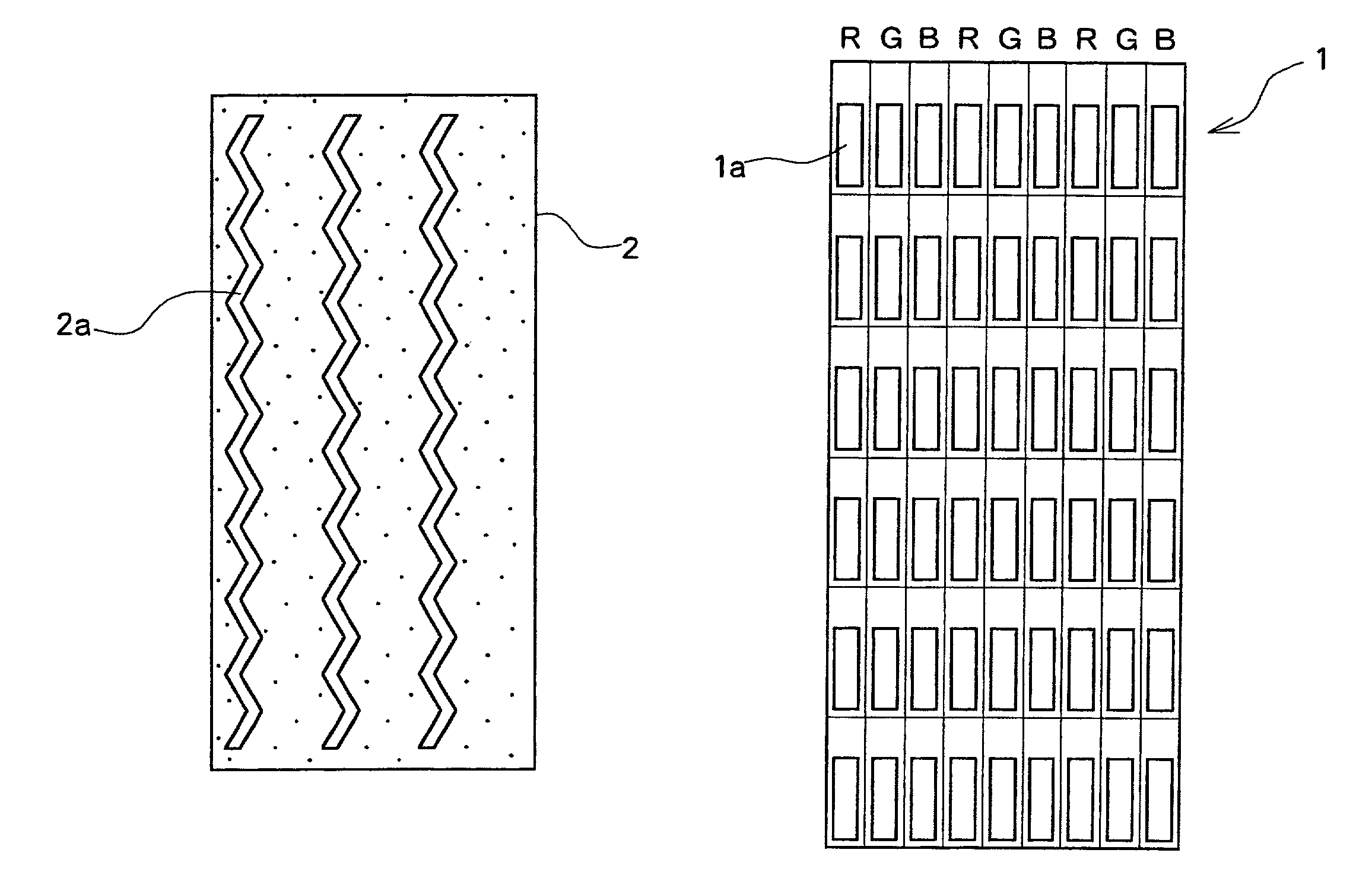
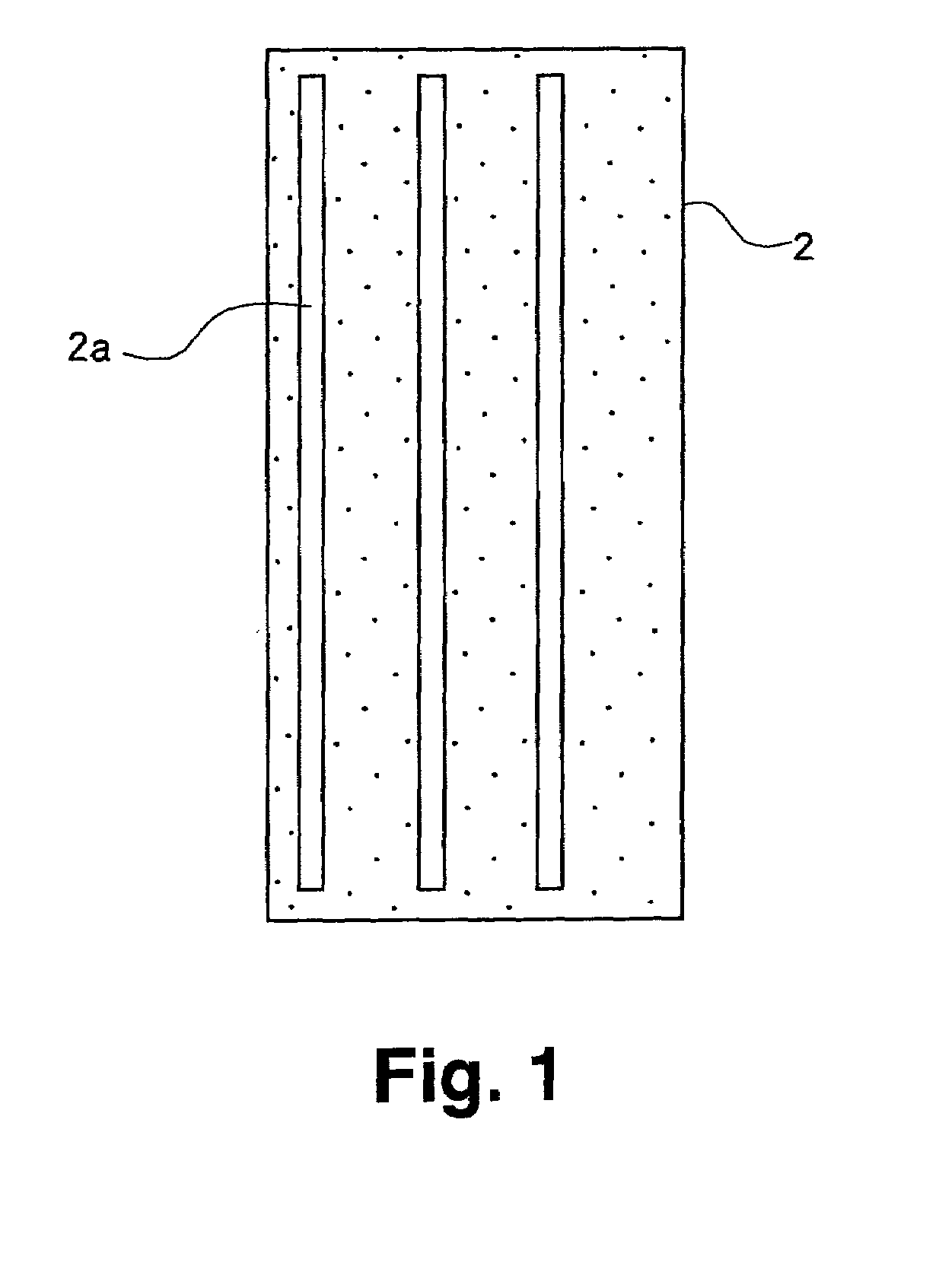
[0036]FIG. 1 shows a configuration of the shadow mask 2 for the formation of the organic emissive layer 63 relating to the present embodiment. In the conventional mask shown in FIG. 9 are discrete openings 2a corresponding to the respective pixels. In the present embodiment are openings 2a that are in common among adjacent pixels. More specifically, for a particular color, the R pixels, for example, the R pixel group is arranged linearly in a column. The opening 2a for forming the R pixels is also arranged linearly in a column so that the opening 2a is in common among adjacent pixels. This yields the opening 2a as a stripe shape as shown in the figure. The width of the opening 2a corresponds to the width of one pixel and the length is determined according to the number of pixels to be in common. Namely, if the organic emissive l...


PUM


Abstract

An organic EL display in which the film thickness of an organic emissive layer is made uniform so as to increase the effective light emission area. An anode and a common cathode are formed for each pixel on the organic EL display. Switching by thin-film transistors causes current to flow between the anode and the cathode so that the organic EL element emits light. The organic EL element comprises a hole transport layer, the organic emissive layer, and an electron transport layer. Among a plurality of pixels disposed in a matrix configuration, the organic emissive layer is formed in common with adjacent pixels of the same color. Forming the organic emissive layer in common can prevent a decrease in the film thickness of the organic emissive layer at the edges of the shadow mask during vapor deposition and result in a uniform film thickness of the organic emissive layer.

Description

BACKGROUND OF THE INVENTION[0001]1. Field of the Invention[0002]The present invention relates to a light-emitting device, and more particularly to increasing the effective light emission area.[0003]2. Description of the Related Art[0004]Flat display panels are recently known to use organic electroluminescence (organic EL) elements. Organic EL elements are self emitting displays in which an electrical current is supplied to an organic EL layer, provided between an anode and a cathode, causing the organic EL layer to emit light. Also since a backlight is unnecessary, unlike LCDs, organic EL elements are expected to be the next major type of flat display panel. In particular, in the active matrix type of organic EL display in which a switching element is formed at each pixel, a larger and higher resolution screen is possible since display data can be stored at each respective pixel.[0005]In this sort of organic EL display, the organic EL layer, which is an emissive layer, is usually fo...

Claims


Application Information

Patent Timeline
IPC IPC(8): H05B33/10H01L27/32H01L51/50H01L51/56H05B33/12
CPCH01L27/3244H01L51/56H10K59/12H10K71/00H05B33/10
Inventor YAMADA, TSUTOMUNISHIKAWA, RYUJI
Owner SANYO ELECTRIC CO LTD
Why Eureka
Try Eureka