Method and apparatus for damping vibrations in a semiconductor wafer handling arm

a technology of handling arm and semiconductor wafer, which is applied in the direction of shock absorbers, mechanical control devices, instruments, etc., can solve the problems of deteriorating positioning accuracy, vibration in the handling arm, and the speed with which the handling arm can position and remove the wafer at high speed,

Inactive Publication Date: 2005-12-20
NOVELLUS SYSTEMS
View PDF13 Cites 14 Cited by
  • Summary
  • Abstract
  • Description
  • Claims
  • Application Information

AI Technical Summary

Problems solved by technology

One limitation on the speed of processing is the speed with which the handling arm can position and remove the wafer from the processing station.
The rapid motion necessary to achieve high speed operation excites vibrations in the handling arm.
If the vibrations are not allowed to dissipate sufficiently, positioning accuracy deteriorates.
In addition, excess vibration results in particle generation due to impacts between the arm and wafer.
This introduces contaminants into the processing chamber.
Existing semiconductor wafer handling arms are not provided with vibration dampers due to the difficulty of finding vibration absorbing materials that are suitable for use in semiconductor processing environments.
This creates a source of contaminants that is unacceptable in the ultra-lean environment needed for semiconductor wafer processing.
This makes them a poor choice for use in such an environment.

Method used


Image

  • Method and apparatus for damping vibrations in a semiconductor wafer handling arm
  • Method and apparatus for damping vibrations in a semiconductor wafer handling arm
  • Method and apparatus for damping vibrations in a semiconductor wafer handling arm

Examples


Embodiment Construction

)

[0028]In describing the preferred embodiment of the present invention, reference will be made herein to FIGS. 1 to 6 of the drawings in which like numerals refer to like features of the invention.

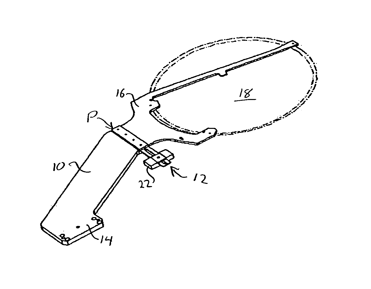
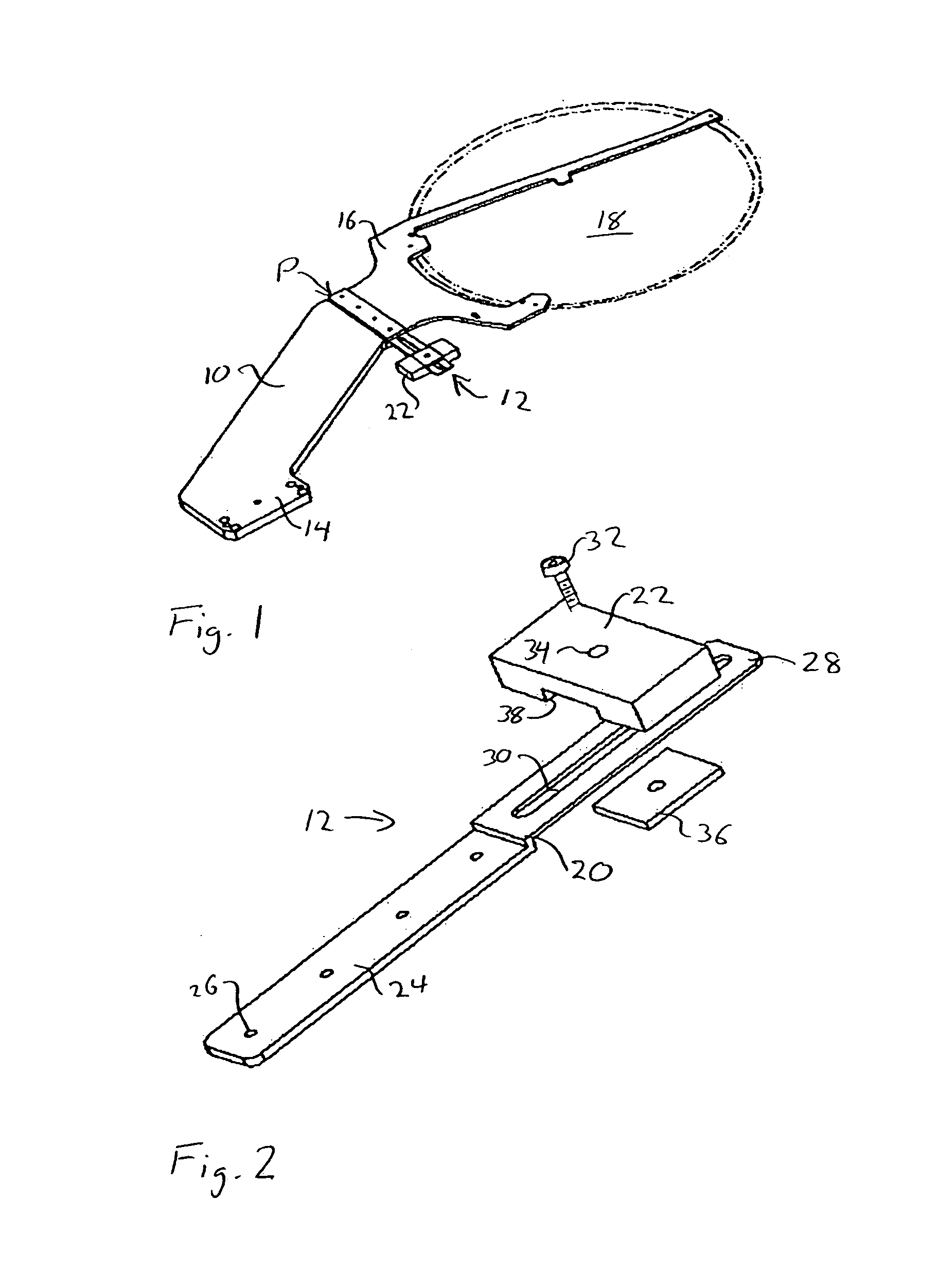
[0029]FIG. 1 illustrates a semiconductor wafer handling arm 10 having a vibration damper 12 according to the present invention attached to the arm 10. The base 14 of the handling arm 10 is provided with a mount for attachment to the driving portion of the transport mechanism (not shown) and the opposite end 16 is provided with a mechanism that holds the semiconductor wafer 18 (shown in phantom).

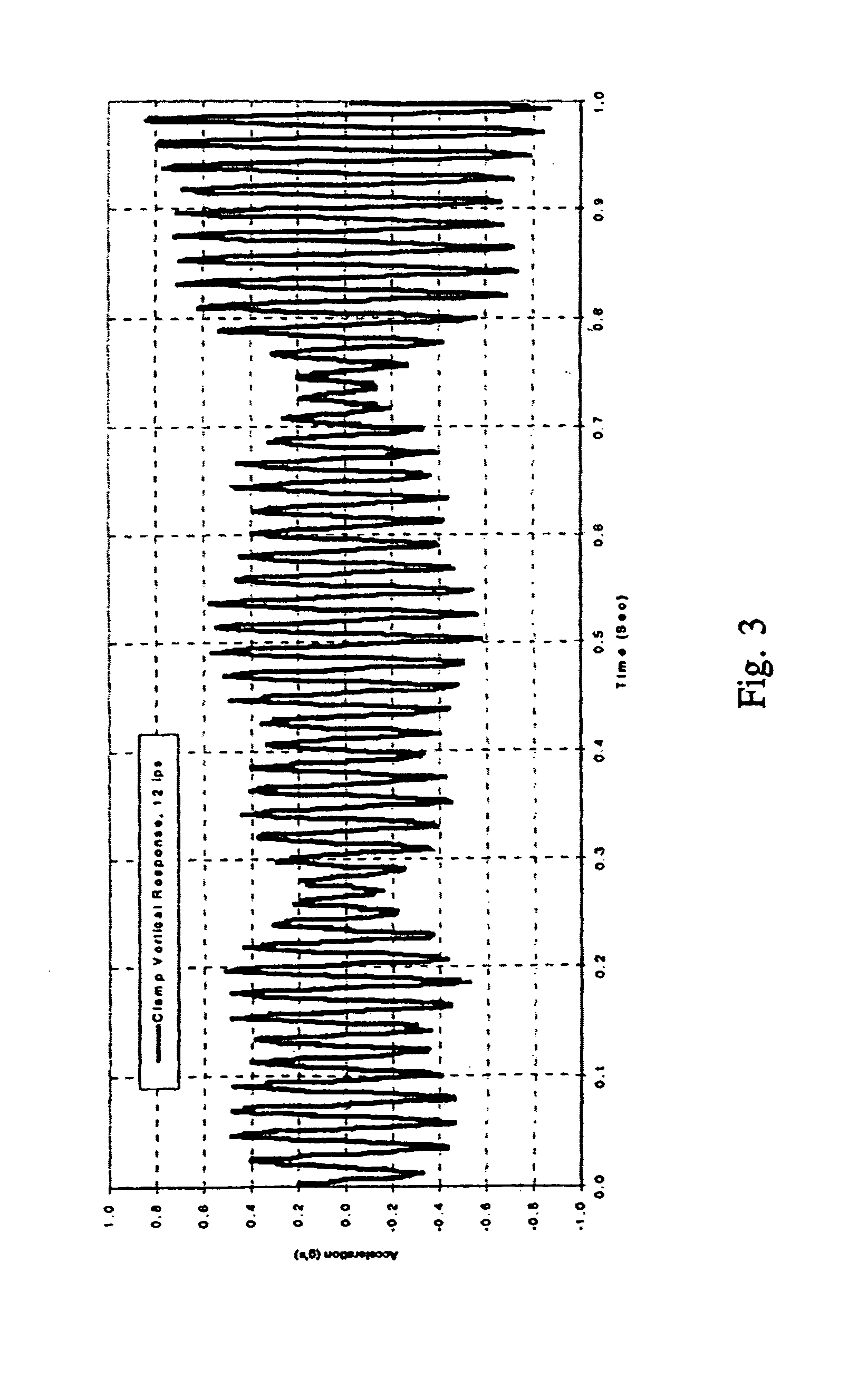
[0030]The wafer 18 defines a plane and the vibrations of greatest concern are vibrations due to the second bending mode in the direction perpendicular to that plane. These “out of plane” vibrations cause impacts between the arm and the wafer that produce contaminant particles. The vibration damper 12 is attached to the arm at point P, which is a high response point for the second bending mode of the...


PUM

PropertyMeasurementUnit
velocityaaaaaaaaaa
timeaaaaaaaaaa
velocityaaaaaaaaaa

Abstract

A method of damping a semiconductor wafer handling arm by attaching a spring and a mass coupled to the spring to form a mass spring system that is tuned to vibrate at a structural resonant frequency of the vibrating wafer handling arm. The spring has temperature insensitive spring characteristics and the mass and spring are constructed of materials that do not outgas or produce contaminants in a semiconductor processing environment. The mass spring system is preferably a cantilever beam spring connected to a high response point on the vibrating arm and oriented to vibrate in a plane perpendicular to the plane of the wafer. The mass is slidably adjustable along the length of the cantilever beam spring to adjust the resonant frequency. Vibration damping of the wafer handling arm is accomplished by the transfer of kinetic energy from the vibrating wafer handling arm to the mass spring system.

Description

[0001]This application is a divisional of U.S. Pat. No. 6,761,085, filed Feb. 6, 2002, now U.S. Pat. No. 6,761,085 patented Jul. 13, 2004.BACKGROUND OF THE INVENTION[0002]1. Field of the Invention[0003]This invention relates to transport mechanisms for rapidly moving and positioning semiconductor wafers. More specifically, this invention relates to methods and devices for damping vibrations in a handling arm used in such a transport mechanism.[0004]2. Description of Related Art[0005]In modern high speed semiconductor manufacturing operations semiconductor wafers are moved into position for processing with an automated transport mechanism. The transport mechanism uses a handling arm to pick up the wafer and move it into the desired position. One end of the handling arm is connected to the driving portion of the transport mechanism and the other end holds the wafer as it is moved.[0006]One limitation on the speed of processing is the speed with which the handling arm can position and ...

Claims


Application Information

Patent Timeline
Patent Type & Authority Patents(United States)
IPC IPC(8): B21D39/03H01L21/677H01L21/687
CPCH01L21/67766H01L21/68707Y10T74/20305Y10T29/49826Y10S414/135
Inventor TAN, MARK
Owner NOVELLUS SYSTEMS
Why Eureka
Try Eureka