

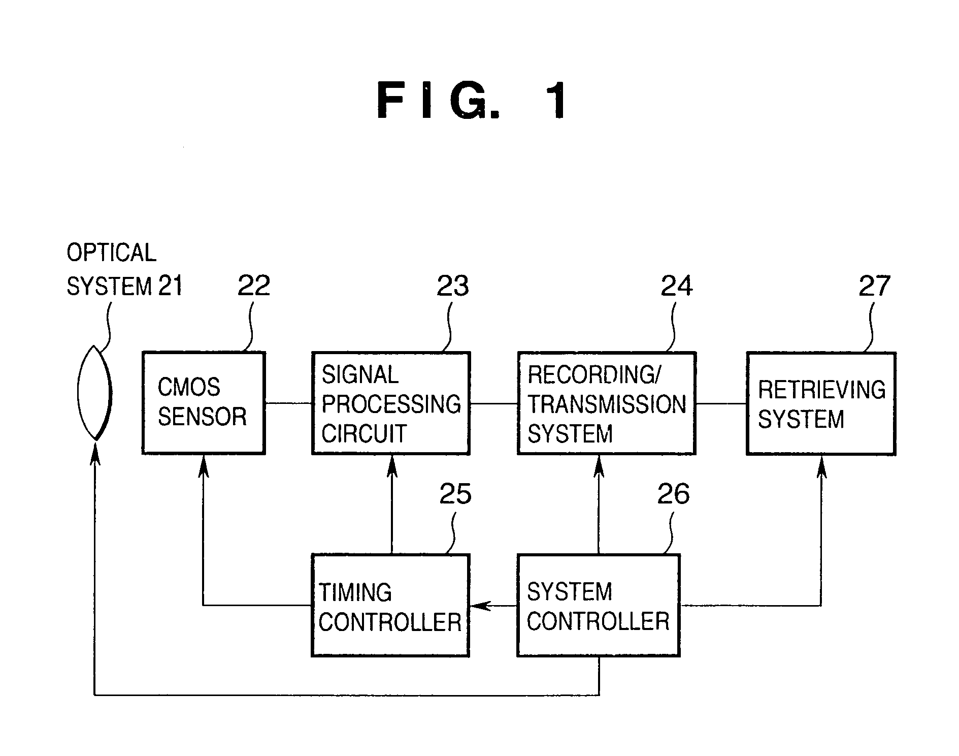
Arrangement of circuits in pixels, each circuit shared by a plurality of pixels, in image sensing apparatus
a technology of image sensing apparatus and circuit, which is applied in the direction of radio frequency control devices, instruments, television systems, etc., can solve the problems of deterioration of the dynamic range, sensitivity, and s/n ratio of an image sensing apparatus, and the practical layout of the foregoing elements on the chip, so as to achieve good performance without deterioration in resolution
- Summary
- Abstract
- Description
- Claims
- Application Information
AI Technical Summary
Benefits of technology
Problems solved by technology
Method used
Image

Examples
first embodiment
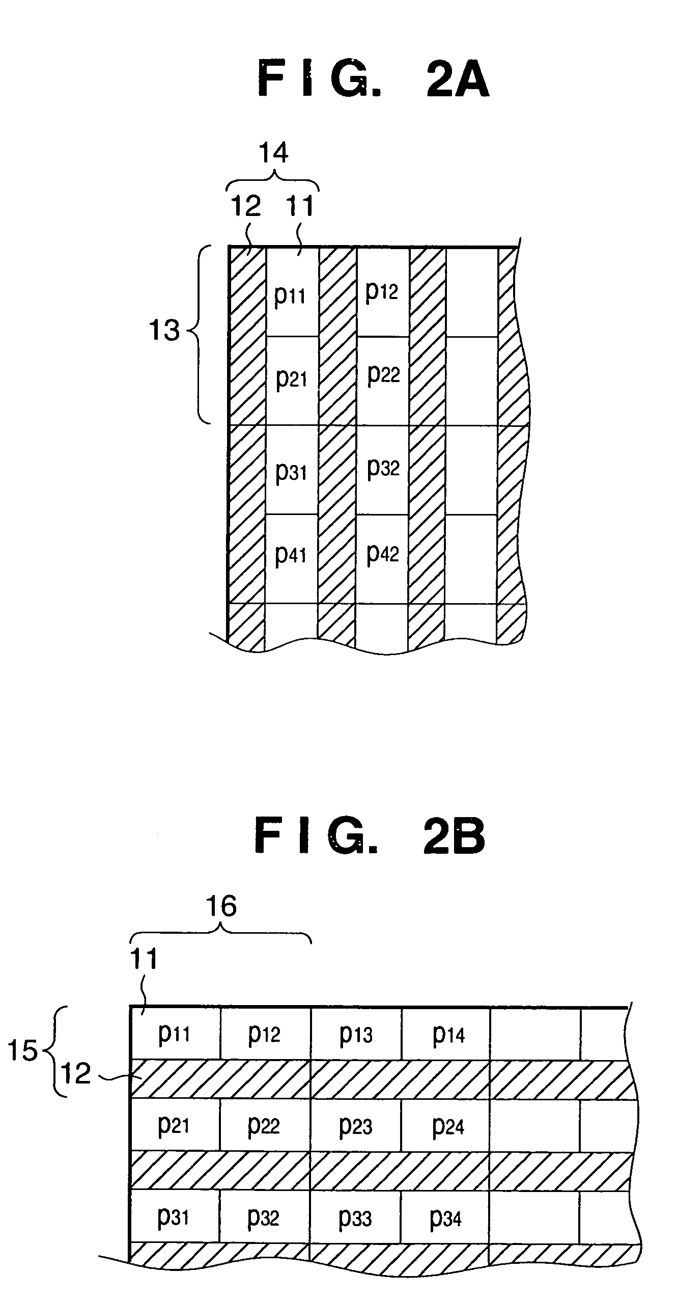
[0095]FIG. 2A shows a layout of amplifiers 12 in pixels when each amplifier 12 is shared by two pixels adjoining in the column direction, and FIG. 2B shows a layout of amplifiers 12 in pixels when each amplifier 12 is shared by two pixels adjoining in the row direction.
[0096]In FIG. 2A, two photoelectric conversion elements 11 (such as, pairs of the elements P11, and P21, P31 and P41, P12 and P22, P32 and P42, and so on) sharing one amplifier 12 are arranged next to each other in the column direction, and the amplifier 12 is arranged along the adjoining pixels. In this manner, intervals between the centers of mass of the photoelectric conversion elements 11 (e.g., P11, P21, P31, P41, P12, P22, P32, P42) in both the row and column directions become equal. Reference numeral 13 indicates a unit cell repeated in the column direction, and reference numeral 14 indicates the unit cell repeated in the row direction.
[0097]Further, in FIG. 2B, two photoelectric conversion elements 11 (such as...
second embodiment
[0139]Next, the second embodiment of the present invention will be explained.
[0140]FIGS. 13 and 14 show other layouts of amplifiers 12, as common circuits, and photodiodes 11 when each amplifier 12 is shared by two photodiodes 11.
[0141]As shown in FIG. 13, the photodiodes 11 are arranged so that adjoining rows are shifted from each other by one half pitch. In odd-number rows, pixels covered by green (G) filter (referred to as “G pixel” hereinafter), which contribute mainly to a luminance (Y) signal, are respectively set across the amplifiers from pixels covered by red (R) filter (referred to as “R pixel” hereinafter), which contribute to a color-difference signal, and in even-number rows, G pixels are respectively set across the amplifiers from pixels covered by blue (B) filter (referred to as “B pixel” hereinafter), which also contributes to a color-difference signal. By arranging the G pixels in adjoining rows, shifted by one and half pitches in the row direction, intervals betwee...
third embodiment
[0168]Next, the third embodiment of the present invention will be explained with reference to accompanying drawings.
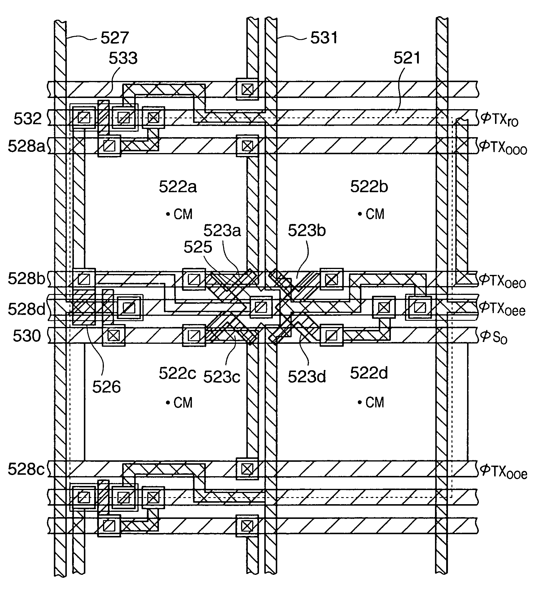
[0169]FIG. 19 shows a layout of amplifiers 12 in pixels when each amplifier 12 is shared by four (2 rows×2 columns) pixels, according to the third embodiment.
[0170]In FIG. 19, each amplifier 12 is arranged in the center of four pixels, and four photoelectric conversion elements 11 (e.g., q11, q12, q21, q22) are arranged as they surround the amplifier 12.
[0171]Further, a light-shield unit 17 is provided for each pixel in an area which is symmetry to a portion of the amplifier 12 occupying the pixel with respect to the center of the pixel. Therefore, the center of mass of each photoelectric conversion element 11 is in the center of each pixel. Accordingly, the centers of mass of the photoelectric conversion elements 11 (q11, q12, q21, q22, q31, q32, q41, q42) are arranged at a same interval, D, both in the row and column directions.
[0172]FIG. 20 shows another layout of a...
PUM
 Abstract
Description
Claims
Application Information