Solid state imaging device for reducing camera size
- Summary
- Abstract
- Description
- Claims
- Application Information
AI Technical Summary
Benefits of technology
Problems solved by technology
Method used
Image
Examples
Embodiment Construction
[0044]This invention will be described in further detail by way of example with reference to the accompanying drawings.
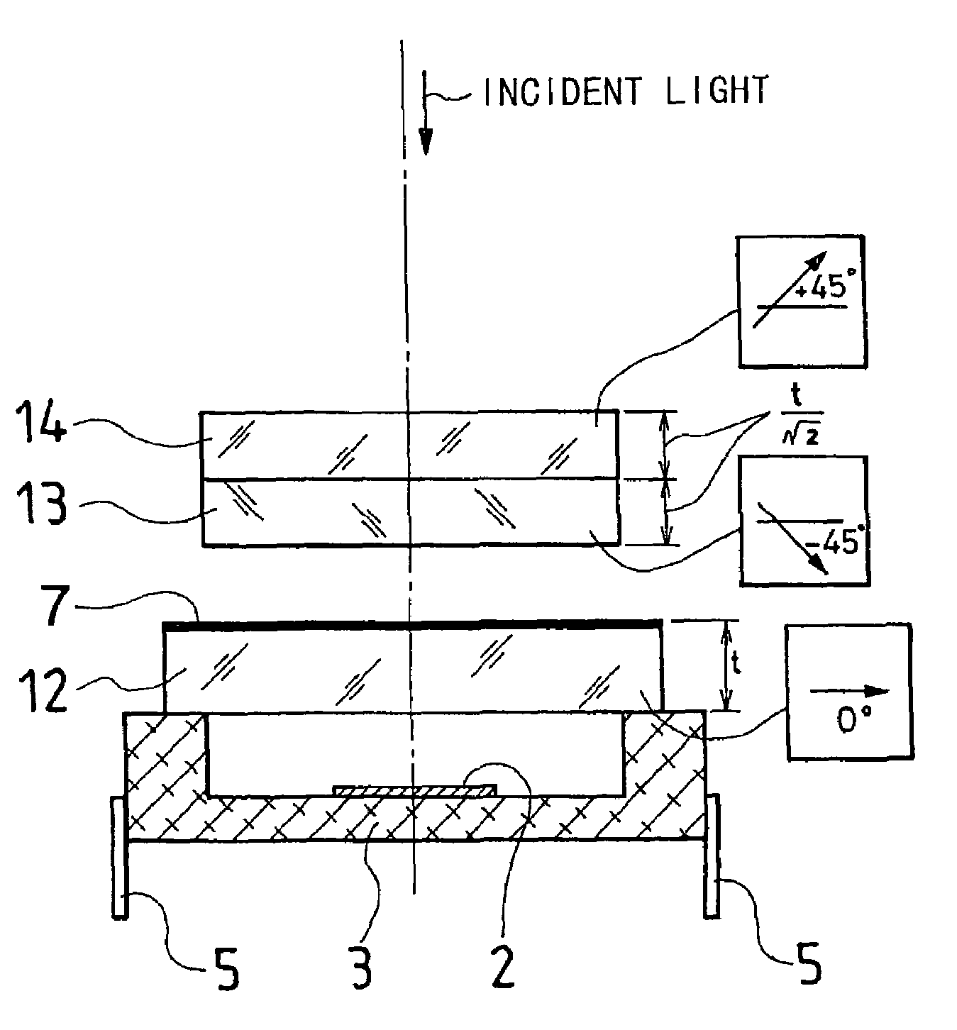
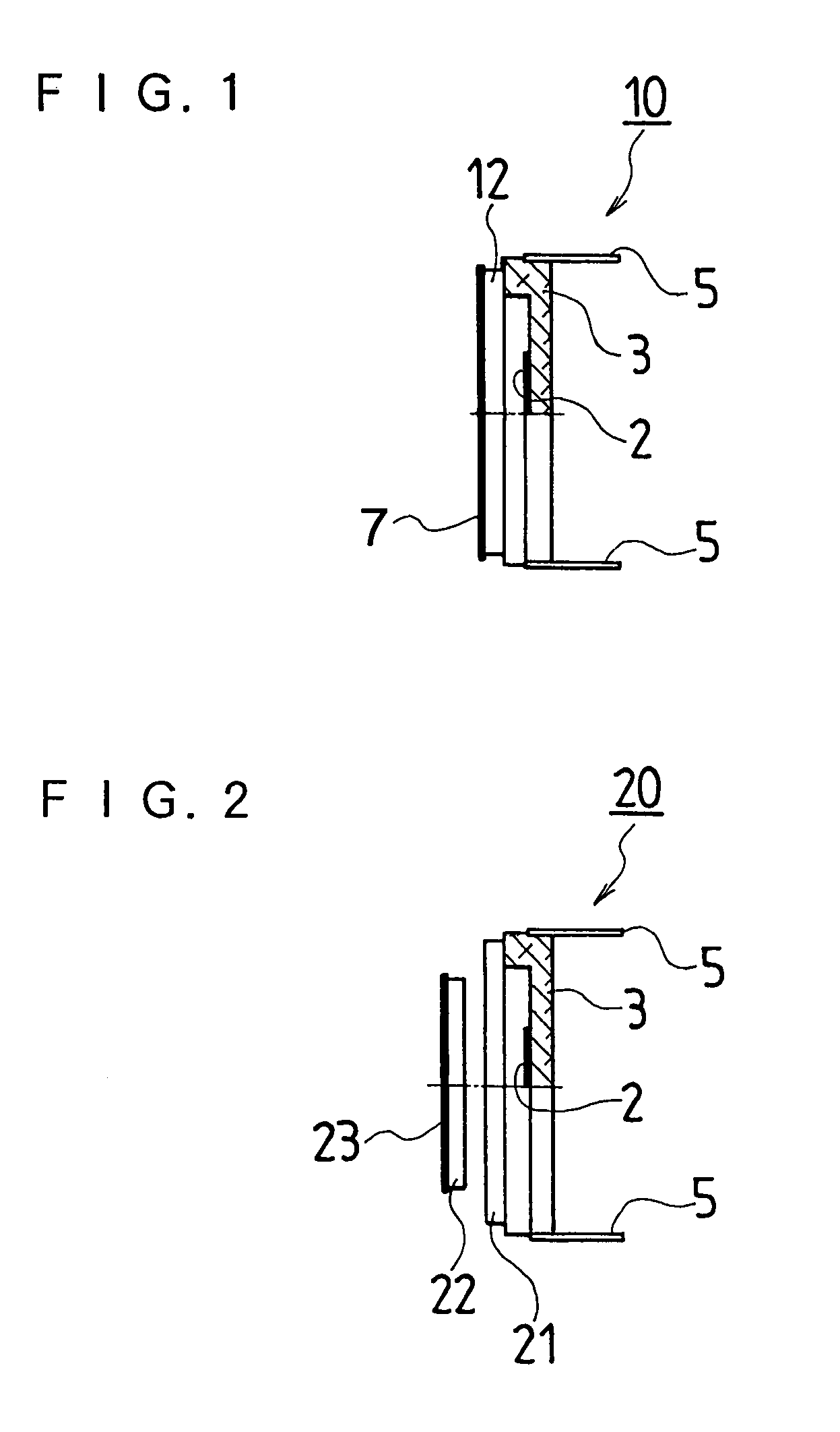
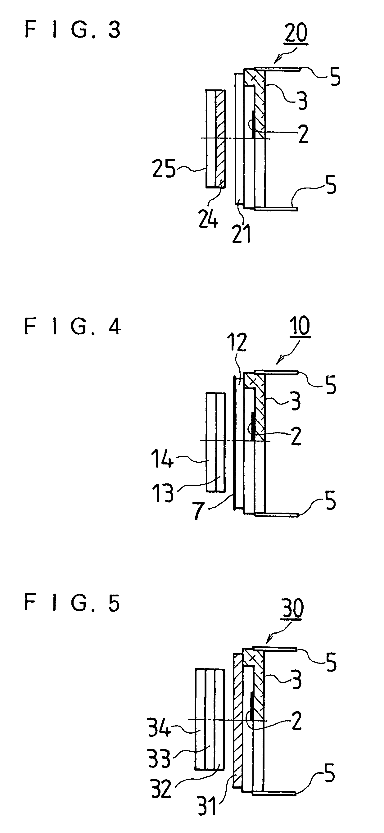
[0045]FIGS. 1–5 show the first through fifth embodiments of a solid state imaging device according to the present invention.
[0046]The solid state imaging devices of the first through fifth embodiments are equivalent to a conventional solid state imaging device 1 shown in FIGS. 19–23. In the solid state imaging devices of the present invention, optical low-pass filters and the like are efficiently arranged instead of the cover glass 4.
[0047]More specifically, a solid state imaging device 10 in FIG. 1 comprises a solid state imaging device chip 2, a package 3 composed of a ceramic plate, etc. with a lead 5, and an optical low-pass filter 12 made of a double refraction substance (an artificial crystal) whose surface is coated with an IR cut coating 7 composed of multilayer film. The solid state imaging device chip 2 is attached to the package 3 and is bonded to the lea...
PUM
 Abstract
Description
Claims
Application Information


