Coherent evanescent wave imaging

a technology of evanescent wave and coherent wave, applied in the field of methods and apparatuses for observing the characteristics of nanostructures, can solve the problems of insufficient nanostructure characteristics, limit observation, and daunting difficulty in characterizing nanostructures based on observation

Inactive Publication Date: 2005-12-27
THE ARIZONA BOARD OF REGENTS ON BEHALF OF THE UNIV OF ARIZONA
View PDF13 Cites 49 Cited by
  • Summary
  • Abstract
  • Description
  • Claims
  • Application Information

AI Technical Summary

Problems solved by technology

There has been considerable interest in understanding and developing nanostructures, but this has been hampered by limitations on observation that these structures impose by nature of their size.
Whereas in the past, various microscopy techniques have been sufficient to detect defects of a surface at the nanostructure level, or the mere presence of a nanostructure, these have been inadequate to provide characteristics of the nanostructure such as would permit development of images or details of physical features, such as dimensions, shape and other characteristics.
One daunting difficulty in characterizing nanostructures based on observation has been the wavelength of light.
This technique is not suitable for imaging nanostructures.
First, the reduction in wavelength is not sufficient to permit imaging of specimens or structures having dimensions of just a few nm.
Second, nanostructures within a liquid are likely to have their observable characteristics and their observable motion altered or distorted.
This would slow the speed of the light by a factor of two, consequently reducing the wavelength by half.
Again, this is both impractical and insufficient.
The nanostructures being examined cannot be situated in a diamond medium, and halving the 488 nm. wavelength is still not a sufficient reduction.
Rather, Maier et al. suggest optical wave guides fashioned into optical path “Ls,”“Ts” and switches for use in optical circuitry, so slowing the speed of light is not an objective.

Method used


Image

  • Coherent evanescent wave imaging
  • Coherent evanescent wave imaging
  • Coherent evanescent wave imaging

Examples


Embodiment Construction

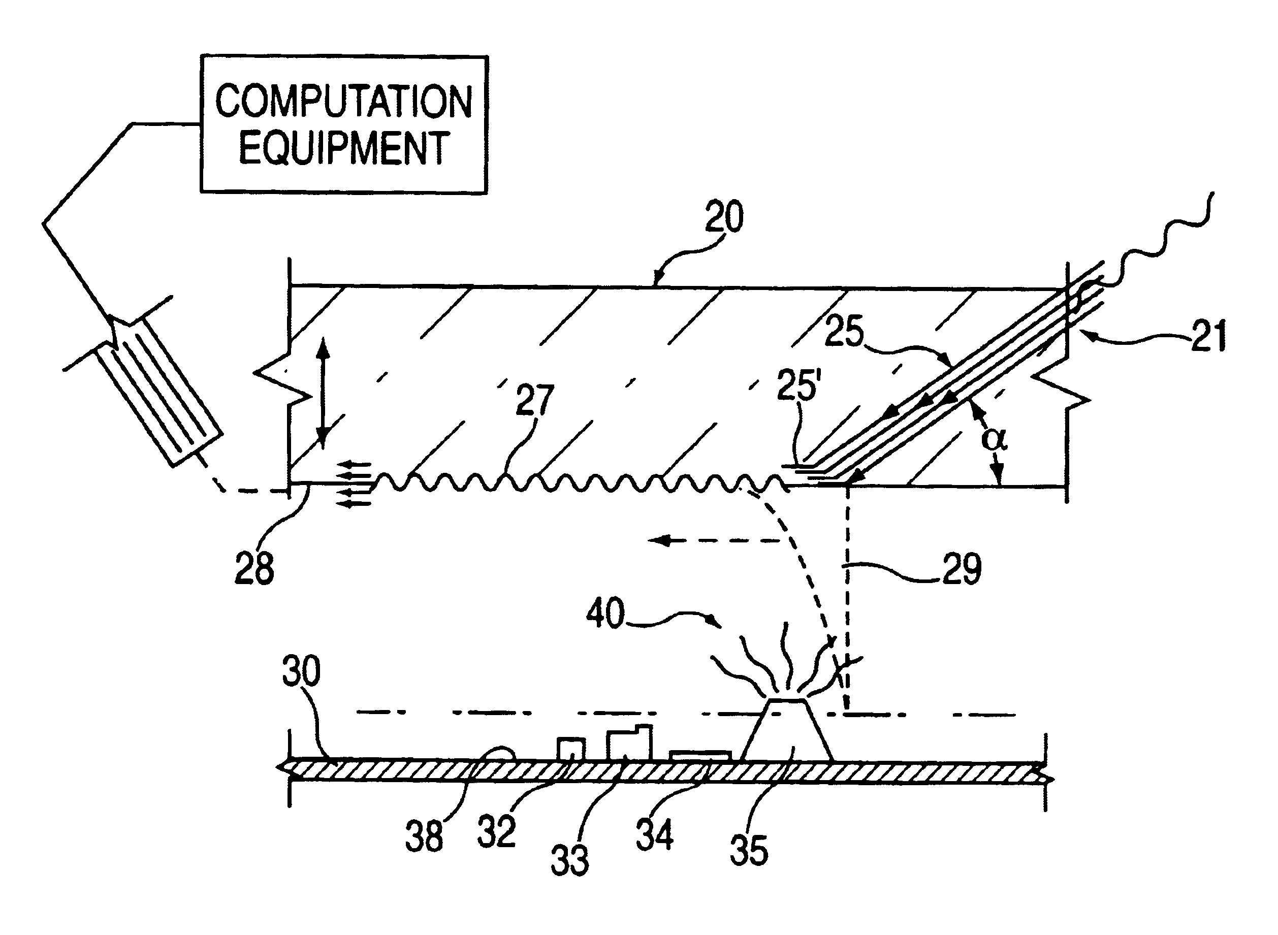
[0023]Turning to FIG. 1, a cross section of a portion of an instrument for detecting physical characteristics of nanostructures is diagrammatically illustrated for purpose of explanation. A surface wave is produced at the surface of a waveguide. The surface wave is an electromagnetic slow wave that does not travel in free space but is bound to a surface. The wave exists at the boundary between a medium (the waveguide) and the free space, air or other medium outside the waveguide boundary. Such a wave has associated with it an exponentially decaying tail located outward of the waveguide in the air or free space bounded by the surface of the guide. The free space portion of the surface wave thus created in the space proximate the waveguide's surface is termed an “evanescent wave.” The wave does not propagate away from the boundary, but it is detectable. It does not radiate, but an object placed in the wave will radiate. As graphically illustrated in FIG. 1, a waveguide 20 is irradiate...


PUM

PropertyMeasurementUnit
distancesaaaaaaaaaa
distancesaaaaaaaaaa
lengthaaaaaaaaaa

Abstract

Methods and apparatus for gathering image information from nanostructures includes a composite waveguide of conductive nanoparticles in a dielectric medium. The waveguide is irradiated with preferably coherent blue light to form a slow surface wave. The evanescent wave that is the “tail” of the surface wave exists outside the waveguide contiguous to its surface. The nanostructures are located to encounter the evanescent wave. The slowing of the wave that occurs in the waveguide reduces the wave's speed and wavelength sufficiently such that nanostructures can be imaged. Upon encountering the evanescent wave, the nanostructures radiate. This radiation causes a backward scattering from the structures and a forward perturbation of the wavefront of the surface wave. From the scattering and perturbation information about the physical characteristics of the nanostructures sufficient to form an image is derived.

Description

RELATED APPLICATIONS[0001]This application is related to and claims priority from U.S. Provisional Application Ser. No. 60 / 280,644 entitled Coherent Evanescent Wave Imaging of Rudolfo Diaz, Ampere Tseng, Karl Booksh, Jose Menendez, Michael Wagner and Sethuraman Panchanathan, filed Mar. 30, 2001.FIELD OF THE INVENTION[0002]This invention relates to methods and apparatuses for observing the characteristics of nanostructures and more particularly methods and apparatus for producing images of nanostructures by causing the nanostructures to encounter a slow, electromagnetic, evanescent wave formed by a slowed electromagnetic surface wave in a waveguide irradiated with electromagnetic energy having a free-space wavelength substantially greater than that of the resultant slow wave in the medium of the wave guide.BACKGROUND OF THE INVENTION[0003]There has been considerable interest in understanding and developing nanostructures, but this has been hampered by limitations on observation that ...

Claims


Application Information

Patent Timeline
Patent Type & Authority Patents(United States)
IPC IPC(8): G01N21/45G01N21/956G02B6/122G02B6/42
CPCB82Y15/00B82Y20/00G01N21/453G01N21/956G02B6/1226
Inventor DIAZ, RODOLFO E.TSENG, AMPERE A.BOOKSH, KARL S.MENENDEZ, JOSEPANCHANATHAN, SETHURAMANWAGNER, MICHAEL
Owner THE ARIZONA BOARD OF REGENTS ON BEHALF OF THE UNIV OF ARIZONA
Why Eureka
Try Eureka