Data output control circuit

a control circuit and data technology, applied in the field of semiconductor memory devices, can solve the problems of increasing the size of the data output control circuit, increasing the power consumption, and increasing the time error between the external clock signal and the internal operating clock signal, so as to reduce the size of the synchronous semiconductor memory device and reduce power consumption

Active Publication Date: 2006-01-03
MOSAID TECH
View PDF4 Cites 37 Cited by
  • Summary
  • Abstract
  • Description
  • Claims
  • Application Information

AI Technical Summary

Benefits of technology

[0048]It is, therefore, an object of the present invention to provide a data output control circuit capable of generating a rising data output enable signal and a falling data output enable signal for reducing power consumption and for decreasing size of a synchronous semiconductor memory device.

Problems solved by technology

When the external clock signal is inputted to the synchronous semiconductor memory device in order to be used as the internal operating clock signal, there occurs a time error between the external clock signal and the internal operating clock signal.
Therefore, size of a data output control circuit is increased and power consumption is also increased.

Method used


Image

  • Data output control circuit
  • Data output control circuit
  • Data output control circuit

Examples


Embodiment Construction

[0058]Hereinafter, a data output control circuit for use in a synchronous semiconductor memory device in accordance with the present invention will be described in detail referring to the accompanying drawings.

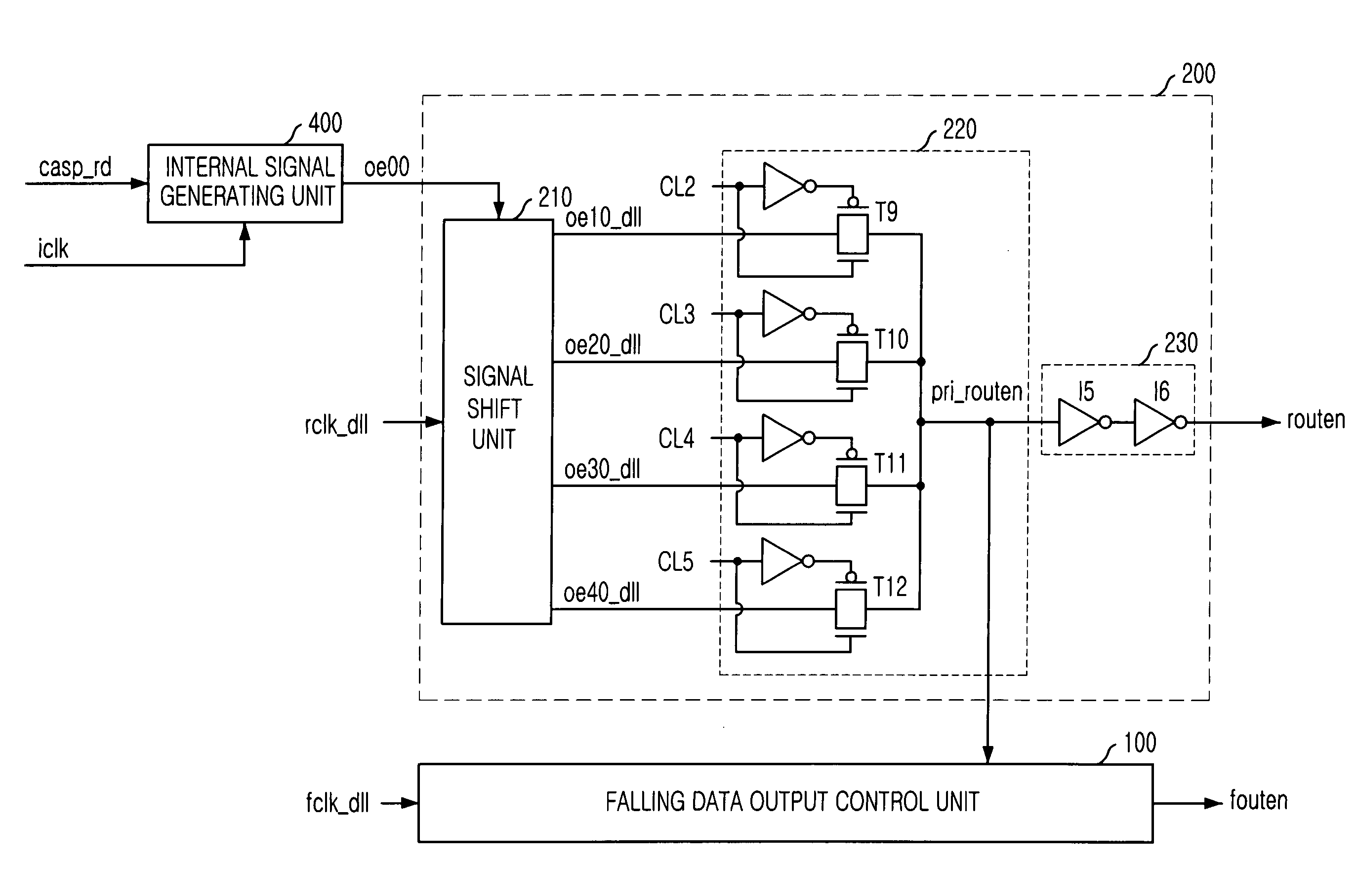
[0059]FIG. 5 is a block diagram showing a data output control circuit in accordance with a preferred embodiment of the present invention.

[0060]As shown, the data output control circuit includes an internal signal generating unit 400, a rising data output control unit 200 and a falling data output control unit 100.

[0061]The internal signal generating unit 400 receives a read command performing signal casp—rd and a clock signal iclk for generating an internal signal oe00 by synchronizing the read command performing signal casp—rd with the clock signal iclk.

[0062]The rising data output control unit 200 receives the internal signal oe00 and a delay locked rising edge clock signal rclk—dll for generating a rising data output enable signal routen in response to a CAS latency (CL).

[0...


PUM


Abstract

A data output control circuit for use in a synchronous semiconductor memory device including: a first data output enable signal generation unit for receiving an internal signal and generating a rising data output enable signal synchronizing with a rising edge of a DLL clock signal according to a CAS latency; and a second data output enable signal generation unit for receiving the rising data output enable signal and generating a falling data output enable signal synchronizing with a falling edge of the DLL clock signal.

Description

FIELD OF INVENTION[0001]The present invention relates to a semiconductor device; and, more particularly, to a data output control circuit for outputting data.DESCRIPTION OF PRIOR ART[0002]A semiconductor memory device has been continuously improved to increase its operational speed. One of methods to improve an operational speed of a semiconductor memory device is to make the semiconductor memory device operate in synchronization with an external clock signal. Therefore, a semiconductor memory device which operates in synchronization with the external clock signal, namely a synchronous semiconductor memory device, has been developed.[0003]The synchronous semiconductor memory device performs a data access operation at a rising edge of the external clock signal. That is, the synchronous semiconductor memory device can perform the data access operation once within one cycle of the external clock signal.[0004]Such a synchronous semiconductor memory device that performs the data access o...

Claims


Application Information

Patent Timeline
Patent Type & Authority Patents(United States)
IPC IPC(8): G11C8/00G11C7/10G11C11/40G11C7/22
CPCG11C7/1051G11C7/1066G11C7/222G11C7/22G11C7/1072G11C11/40
Inventor NA, KWANG-JIN
Owner MOSAID TECH
Why Eureka
Try Eureka