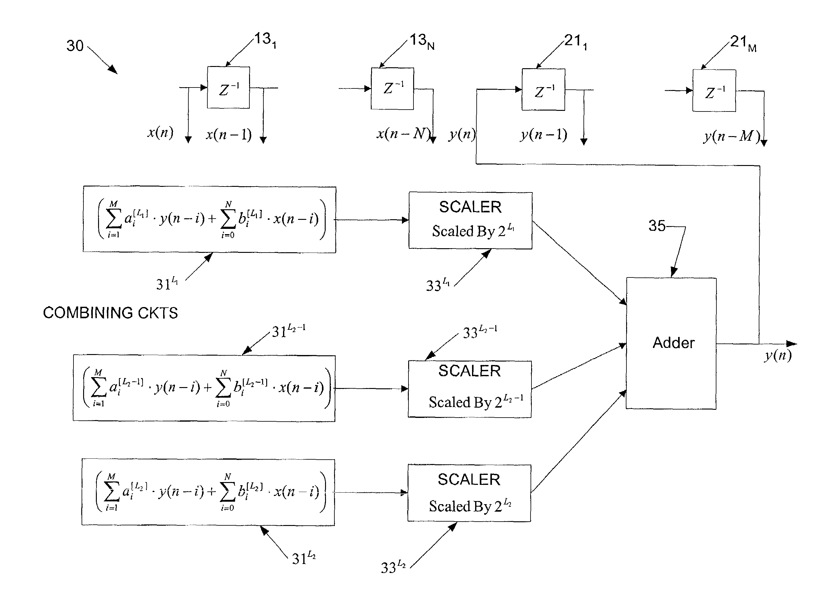
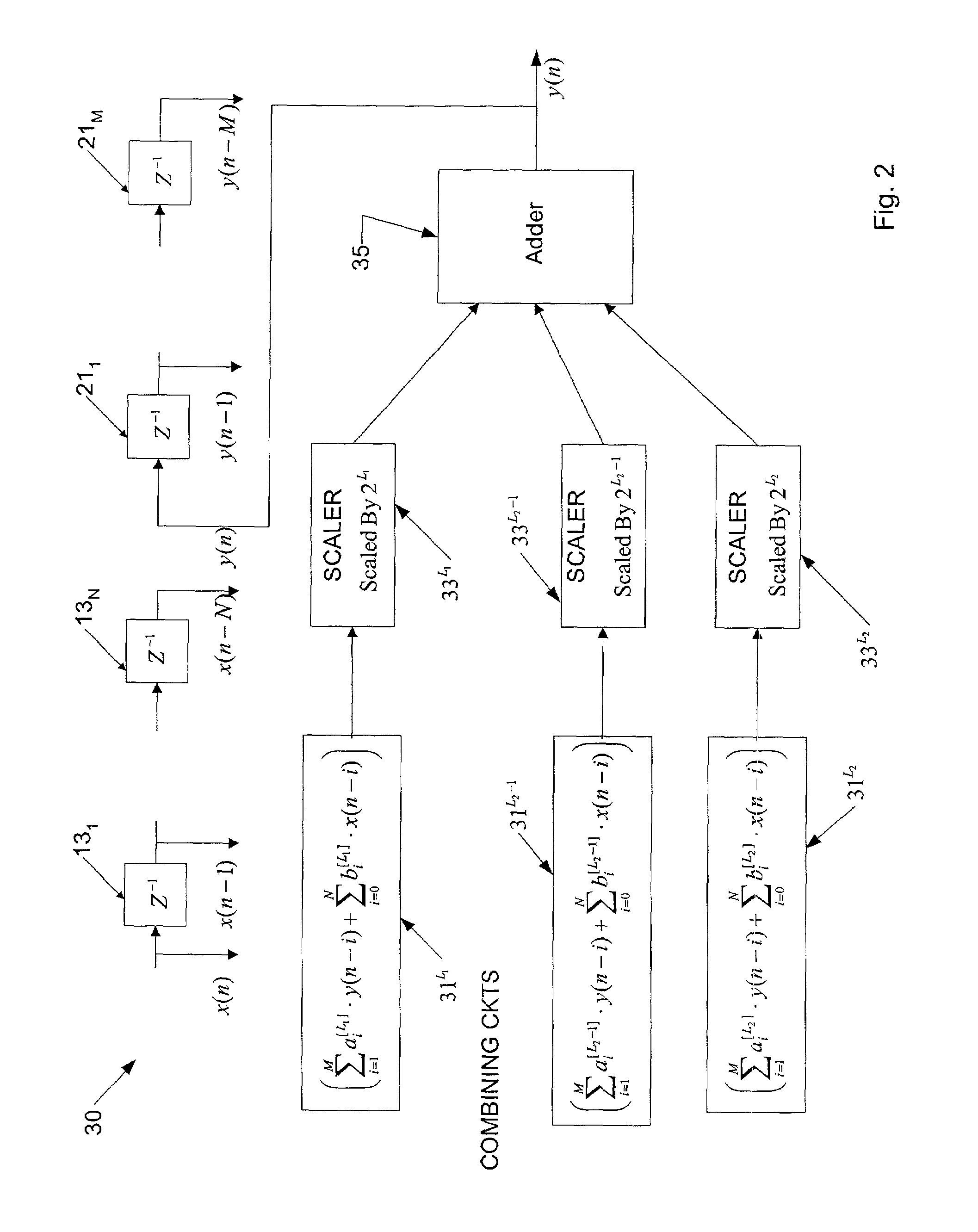
[0032]The present invention relates to an implementation of a digital filter, using selective combining of sample values and scaling of the combined values, to eliminate numeric multiplications, which otherwise might require fixed-point digital multiplications.
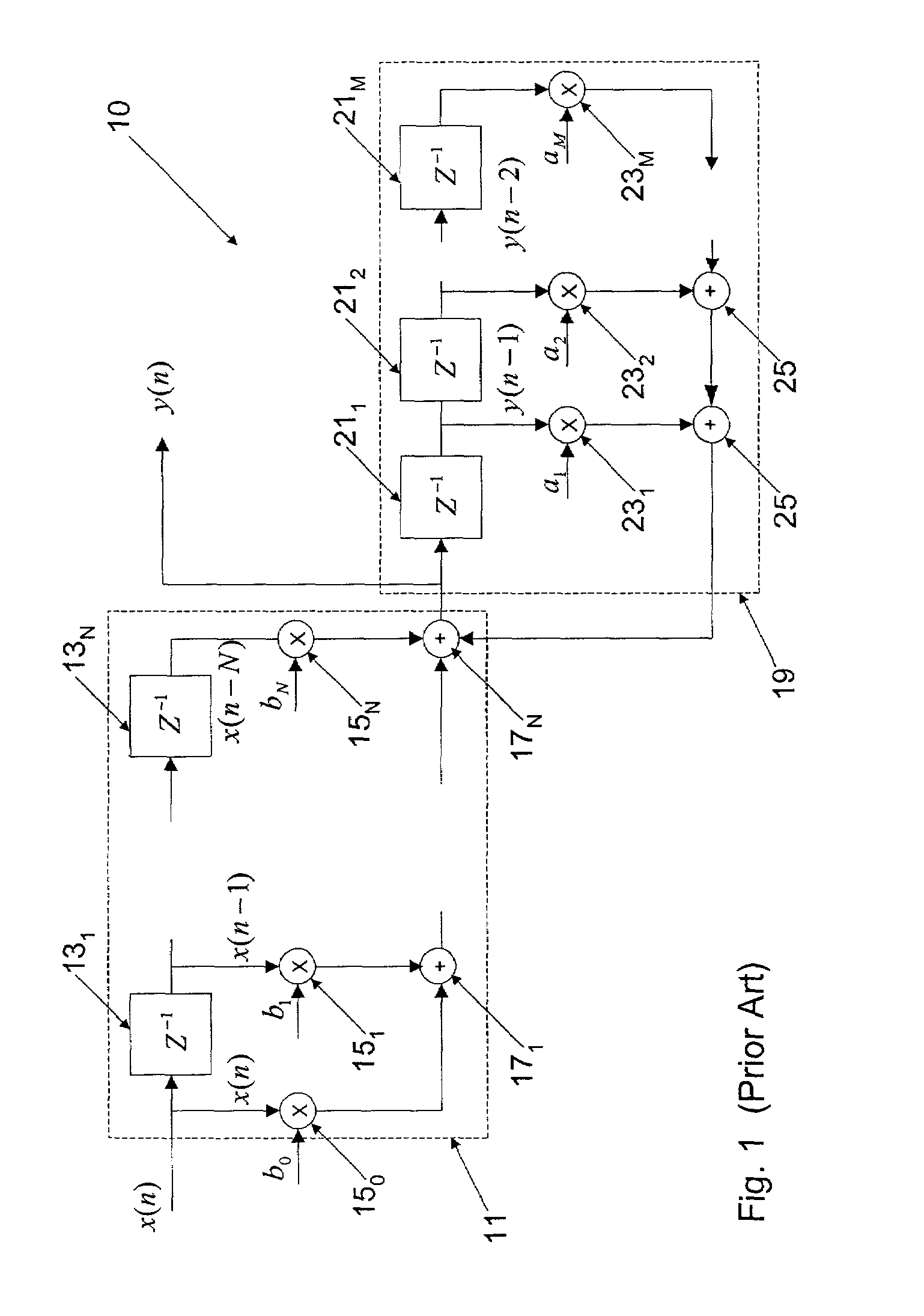
[0033]To appreciate the invention, and how it operates, it may be helpful to first consider the transfer function of a digital filter. As noted above, a digital filter function can be written in the following form: y ( n ) = ∑ l = 1 M a l · y ( n - i ) + ∑ l = 0 N b l · x ( n - i ) ( 1 )
[0034]In a fixed-point implementation of the digital filter, the coefficient values of ai and bi must be in or be converted approximately into the form of: ∑ j = L 1 L 2 c j 2 j ( 2 )
wherein L1 and L2 are two integers, such that:
2L 2 ≧a1≧2L 1 , for i=1, . . . , M
2L 2 ≧b1≧2L 1 , for i=1, . . . , N (3)
[0035]In the equation (2), cj=0 or 1, that is to say a binary 1 or 0 value. Hence, it is possible to eliminate the use of multipliers by using the 0 or 1 binary value and scaling by appropriate powers of 2. With this inventive approach, ai and bi can be expressed in the form of: a l = ∑ j = L 1 L 2 a l [ j ] · 2 j ( 4 ) b l = ∑ j = L 1 L 2 b i [ j ] · 2 j ( 5 ) [0036] wherein ai[j] and bi[j] are 1 or 0 (binary).
[0037]With these notations, we can substitute the summation values (Equations (4) and (5)) for ai and bi values and regroup the common scaling factors and summations, so to as to rewrite the digital filter function y(n) from Equation (1) into the form: y ( n ) = ∑ j = L 1 L 2 ( ∑ i = 1 M a l ( j ) · y ( n - i ) + ∑ l = 0 N b l [ j ] · x ( n - i ) ) · 2 j ( 6 )
[0038]With this form of the filter function, it is then possible to use an appropriate set of scalers, implemented as shift registers for shifting values by the appropriate number of bits positions, for each of the values of j from L1 to L2, rather than using actual multipliers. For each value j, the scaler shifts the binary sum of the components within the parenthesis a number of places equal to j.
[0039]In a general form, the inventive digital filter can be implemented in hardware or as a process flow of a digital signal processor (DSP) as shown in FIG. 2. In a DSP, each functional block comprises one or more processing steps to implement the illustrated function. For discussion purposes, however, assume that the functions shown in FIG. 2 are implemented in hardware. As shown in the drawing, the digital filter 30 includes a delay line comprised on N delay elements 131 to 13N. The delay elements 131 to 13N provide delayed samples of the input signal x(n), as in the filter of FIG. 1. The digital filter 30 also includes a delay line comprised on M (typically N+1) delay elements 211 to 21M, which provide delayed samples of the output signal y(n), as in the filter of FIG. 1.
[0040]The digital filter 30 includes a number of sample-value combining circuits 31 and a corresponding number of shift or scaler circuits 33. Specifically, the digital filter includes combining circuits 31L 1 to 31L 2 . These combining circuits receive appropriate ones of the samples from the input signal x(n), the taps between the delay elements 131 to 13N and/or the taps between the delay elements 211 to 21M, to provide each predetermined set of values for the desired fixed point mathematical combination function.
[0041]It should be noted, however, that the values for the coefficients a and b are binary values 1 and 0. As such, wherever a coefficient is binary 0, in one of the desired filter function sequences, the particular combining circuit 31 does not need to receive the particular sample from the input tapped delay line or the output tapped delay line. Where the coefficient value is a 1, identity, the particular combining circuit 31 simply receives the appropriate sample from input tapped delay line or the output tapped delay line and adds the value to the others in the particular string. Hence, the implementation of each of the circuits 31 requires only appropriate connection to the input signal x(n), the taps between the delay elements 131 to 13N and/or the taps between the delay elements 211 to 21M, and a sufficient number/configuration of adders to sum the particular digital values.
[0042]Each of the combining circuits 31L 1 to 31L 2 outputs the resultant computed value (interim total), as an input sample value for processing by a corresponding one of the scalers 33L 1 to 33L 2 . For each respective integer value L1 to L2, the respective one of the scaler circuits 33L 1 to 33L 2 shifts the binary value from the corresponding one of the combining circuits 31L 1 to 31L 2 by a number of bits or places equal to the respective value of L, to effectively multiply the respective input by the base value (2 in a binary system) raised to the corresponding powers in the range L1 to L2. The scalers 31 may be implemented by shift registers or other simpler digital shift circuits.
[0043]The scalers 33L 1 to 33L 2 supply the scaled values to an adder 35, which totals all of the scaled values to form the output signal y(n). During each clock cycle, the output value y(n) is a computed sample value derived by the computations performed by the digital filter circuit 30, in accordance with the desired filter function and implemented in accordance with the the illustrated example.
[0044]Those skilled in the art will recognize that the digital filter processing, implemented in hardware in FIG. 2, may easily be implemented in the process flow of a digital signal processor, for example by appropriate programming of a digital signal processor.
[0045]Actual application of the inventive filter, for example, in a spread spectrum receiver may be used to approximate a filter function (Equation (1)) that otherwise might require 24 or even 60 multiplications. To appreciate the application and advantages of the inventive concept, however, it may be helpful to consider a very simple example. For that purpose, consider the following filter function.
y(n)=0.875·y(n−1)+0.375·x(n)
[0046]FIG. 3 shows the normal process flow for this simple filter function, if implemented in a manner similar to the circuit of FIG. 1. As shown, the hardware 40 for implementing this simple filter function supplies the current value x(n) sampled from the input signal to a first fixed-point multiplier 150. The multiplier 150 multiplies the current value x(n) by the binary representation of the coefficient value 0.375. The multiplier 150 supplies the product of this multiplication to one input of an adder 17.
[0047]The output of the adder 17 represents the output y(n) of the filter circuit 40. The output y(n) of the filter circuit 40 is applied to a single delay element 211, which is part of a feedback loop. The delay element 211, provides a delay of one cycle, hence the current output of the delay element 211 is the filter output value from the immediately preceding clock cycle, that is to say the value y(n−1). The delay element 211 supplies the value y(n−1) to a multiplier 231, which multiplies the delayed output value y(n−1) by the binary representation of the coefficient value 0.875. The multiplier 231 supplies the product of this second multiplication to the second input of the adder 17, for addition to the current product of the sample x(n) multiplied by the coefficient 0.375 produced by the multiplier 150. As noted, the sum of these two products accumulated by the adder 17 represents the current output value y(n).
[0048]Although the circuit 40 of FIG. 3 appears relatively simple, when illustrated in block diagram form, an actual implementation on an electronic circuit chip is actually relatively complex. Even this simple filter implementation requires two fixed-point numerical multipliers 150 and 231, for multiplying sample values. The more bits included in the sample values, the larger and more complex these multipliers become. The multipliers require a large number of gates, occupy considerable chip-space and consume a large amount of power.
[0049]The multiplications are implemented by a series of adders and scalers. In this example, because
0.875=1·2−1+1·2−2+1·2−3 [0050] we can write 0.875·y(n−1) in the form
y(n−1)·2−1+y(n−1)·2−2+y(n−1)·2−3
[0051]Therefore, 2 adders are needed. Similarly, because
0.375=0·2−1+1·2−2+1·2−3
0.375·x(n)=x(n)·2−2+x(n)·2−3 [0052] 1 adder is needed.
[0053]There is 1 more adder used to combine 0.875·y(n−1)+0.375·x(n), and therefore by a direct method, there are 4 adders needed to implement
y(n)=0.875·y(n−1)+0.375·x(n)
[0054]In accordance with the present concepts, it is possible to replace the fixed-point multiplications of sample values with simple connections corresponding to binary (1 or 0) coefficient values in combination with appropriate scaling operations. Consider now an application of the technique to the same filter function. First, the coefficients 0.875 and 0.375, from the simple example can be expressed in binary form as follows.
0.875=1·2−1+1·2−2+1·2−3
0.375=0·2−1+1·2−2+1·2−3
[0055]By substituting these binary values for the coefficients in the filter function
y(n)=0.875·y(n−1)+0.375·x(n)
the expression for the filter function becomes
y(n)=(1·2−1+1·2−2+1·2−3)·y(n−1)+(0·2−1+1·2−2+1·2−3)·x(n).
[0056]It is then possible to regroup the sample values based on the common scaler functions (powers of 2). This converts the filter function to the expression shown below.
y(n)=(1·y(n−1)+0·x(n))·2−1+(1·y(n−1)+1·x(n))·2−2+(1·y(n−1)+1·x(n))·2−3
[0057]The actual implementation requires three scaling operations (2−1, 2−2 and 2−3) and a corresponding frontend combining circuit to supply the appropriate combinations of samples for the respective scalings. Where the binary coefficients are 0, however, there is no need to process the sample values, and it is possible to eliminate any x or y values multiplied by 0 from the expression. Also, the applications of the 1 coefficients represent multiplications by identity and reduce to the respective sample values for y or x, which can be implemented by simply connecting the appropriate sample values through the combining circuit(s). As a result, the pervious version of the exemplary filter function can be simplified to:
y(n)=y(n−1)·2−1+(y(n−1)+x(n))·2−2+(y(n−1)+x(n))·2−3
[0058]There is 1 adder needed for y(n−1)+x(n); and 2 adders needed to combine y(n−1)·2−1, (y(n−1)+x(n))·2−2 and (y(n−1)+x(n))·2−3 together. Therefore, 3 adders are needed to implement y(n−1)·2−1+(y(n−1)+x(n))·2−2+(y(n−1)+x(n))·2−3. We save 1 adder compared with the direct method. This is a very simple example. In many real digital filters, many more bits and many more multipliers would be required, and therefore the savings on hardware due to use of the invention present teachings is huge. This inventive filter function can be implemented in a digital signal processor or in hardware. FIG. 4 shows a functional representation of the inventive filter processing. These functions may be implemented as process steps performed in the digital signal processor. For discussion of a presently preferred embodiment, the block diagram represents a hardware implementation 50 of this simple digital filter function in accordance with an example.
[0059]As shown, the digital filter 50 comprises only two adders 51, 53, one delay element 55 and three scalers 57, 59 and 61 implemented by shift circuits such as shift registers. The first adder 51 forms the sum of the input value x(n) and the feedback of the delayed output value y(n−1) from the delay element 55.
[0060]The first circuit 57 shifts the input applied thereto one binary place, to scale that input value by 2−1. The second circuit 59 shifts the input applied thereto two binary places, to scale that input value by 2−2. The third circuit 61 shifts the input applied thereto three binary places, to scale that input value by 2−3. The input connections to the shift circuits and the adder 51 perform the functions of the combiner circuits 31 in the embodiment of FIG. 2 to supply the appropriate combined values as inputs to the shift circuit type scalers 57, 59 and 61.
[0061]In this example, the first shift circuit 57 receives the delayed output value of the previous clock cycle y(n−1) and shifts that sample value one binary place, to scale that value by 2−1. The second shift circuit 59 receives the numerical value that is the sum of the delayed output value of the previous clock cycle y(n−1) and the input sample x(n) for the current clock cycle, and the second shift circuit 59 shifts that sum two binary places, to scale that total numerical value by 2−2. In this example, the third shift circuit 61 receives the numerical value that is the sum of the delayed output value of the previous clock cycle y(n−1) and the input sample x(n) for the current clock cycle, and the third shift circuit 61 shifts that total numerical value three binary places, to scale that value by 2−3.
[0062]The second adder 53 sums the scaled outputs of the three shift circuits 57, 59 and 61 to form the overall filter output value y(n), which is also input to the delay device 55 for use in the feedback processing during the next clock cycle.
[0063]The implementation shown in FIG. 4 has been described as a device constructed of appropriate circuit elements. Those skilled in the art will recognize, however, that it is a simple matter to implement the illustrated processing functions as a series of process steps programmed into a digital signal processor.
[0064]The digital filter of the present invention finds particularly advantageous application in digital wireless receiver devices, for example in spread-spectrum receivers of portable wireless terminals. FIG. 5 is a simplified block diagram of such a receiver.
[0065]As shown, the receiver 70 includes an antenna 71 for receiving a spread-spectrum signal transmitted over the air-link. An RF frontend system 72 provides low noise amplification and automatic gain control (AGC) processing of the analog signal from the antenna 71.
[0066]The RF frontend system 72 supplies the channel signal to two translating devices 73 and 74. A local oscillator generates proper carrier-frequency signals and supplies a cos(ωot) signal to the device 73 and supplies a sin(ωot) signal to the device 74. The translating device 73 multiplies the amplified over-the-air channel signal by the cos(ωot) signal; and the translating device 74 multiplies the amplified over-the-air channel signal by the sin(ωot) signal. The translating devices 73 and 74 thereby translate the received multi-channel spread-spectrum signal from the carrier frequency to in-phase (I) and quadrature (Q) signals at a processing frequency.
[0067]The translating device 73 downconverts the in-phase (I) spread-spectrun signal to the processing frequency and supplies the converted signal to an analog to digital (A/D) converter 75. Similarly, the translating device 74 downconverts the quadrature (Q) spread-spectrum signal to the processing frequency and supplies the converted signal to an analog to digital (A/D) converter 76. Each of the digital output signals is applied to a digital filter 30I or 30Q. Each digital filter 30 utilizes the inventive digital filtering technique, in essentially the manner described above relative to FIG. 2, that is to say implemented without numerical value mutiplications. The filters 30I or 30Q may implement substantially the same filter functions or somewhat different filter functions, as appropriate to process the in-phase (I) and quadrature (Q) spread-spectrum signals.
[0068]The filters 30I and 30Q supply filtered output streams of digitized values, representing the received in-phase (I) and quadrature (Q) signals, to further circuitry represented as a direct sequence spread spectrum demodulator and processing circuit 77. The circuit 77 processes the I and Q data streams to recognize code sequences and recover received data and signaling information. The circuit 77, for example, may include matched filter banks for code detection and a processor, which performs interference cancellation, AFC and phase rotation. Such an implementation of the circuit 77 would further include a Rake combiner and decision/demapper circuit 51, to recover and remap the chip sequence signals from the I and Q channels to the original data sequences. The data sequences for the I and Q channels also are multiplexed together to form an output data stream, which is applied to a deinterleaver and then to a decoder, which performs forward error correction. The data and/or signaling information recovered in this manner may be specifically addressed to the particularly receiver 70 or broadcast to a plurality of such receivers.
[0069]A more detailed description of a direct sequence communication system, incorporating a receiver of the type shown in FIG. 5, may be found in commonly assigned U.S. patent application Ser. No. 09/662,148, filed Sep. 15, 2000. The inventive digital filter may also find application in a wide range other spread-spectrum receivers, such as that used in the common packet channel (CPCH) system disclosed in U.S. Pat. No. 6,169,759 to Kanterakis et al. or in the system disclosed in commonly assigned U.S. patent application Ser. No. 09/570,393 filed May 12, 2000. The disclosures of the commonly assigned applications and the 6,169,759 Patent are incorporated entirely herein by reference.
[0070]Those skilled in the art will recognize that the present invention has a broad range of applications, for example, in digital filter processing applications for various other wired and wireless telecommunications receivers and for many other digital signal processing purposes. The invention also admits of a wide range of modifications without departure from the inventive concepts. For example, the embodiments described above utilized binary or base 2, however, the invention may be implemented in base 4 or in other numerical systems.
[0071]While the foregoing has described what are considered to be the best mode and/or other preferred embodiments of the invention, it is understood that various modifications may be made therein and that the invention may be implemented in various forms and embodiments, and that it may be applied in numerous applications, only some of which have been described herein. It is intended by the following claims to claim any and all modifications and variations that fall within the true scope of the inventive concepts.