Semiconductor device
- Summary
- Abstract
- Description
- Claims
- Application Information
AI Technical Summary
Benefits of technology
Problems solved by technology
Method used
Image

Examples
Embodiment Construction
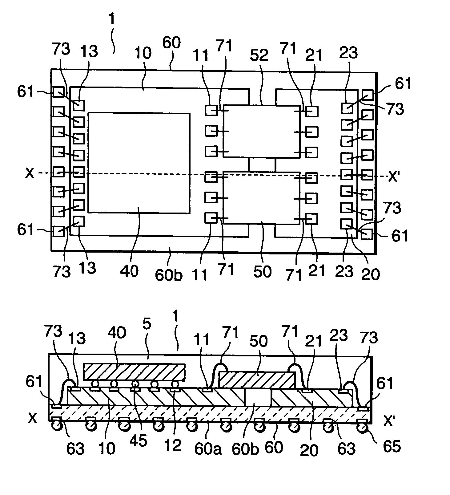
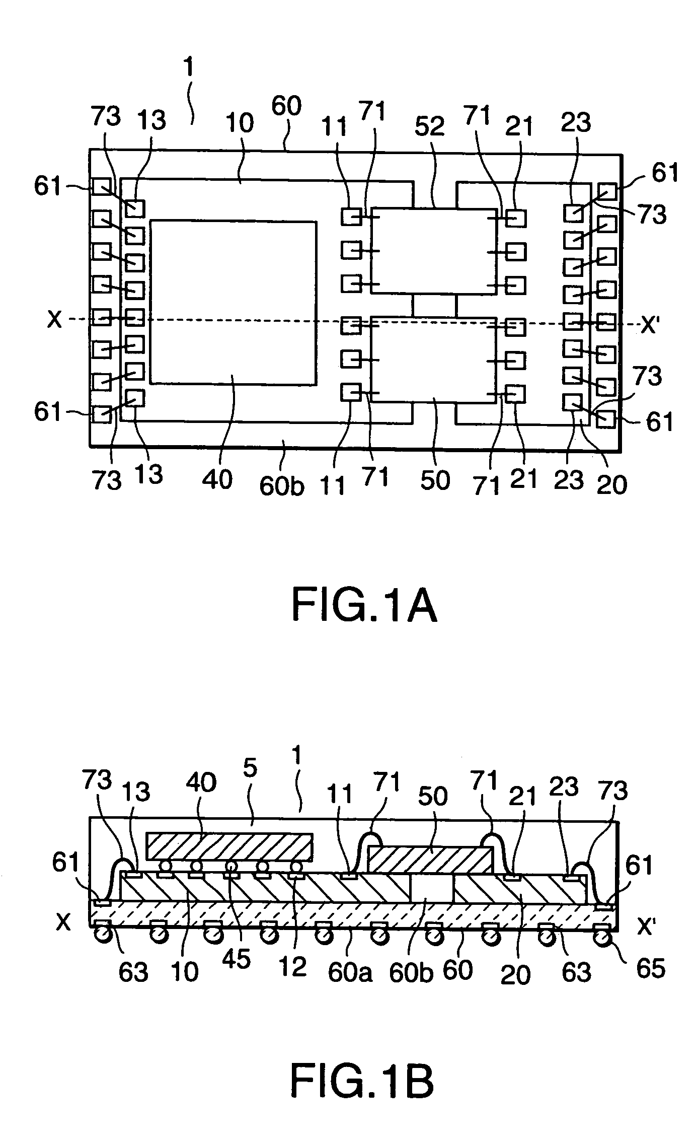
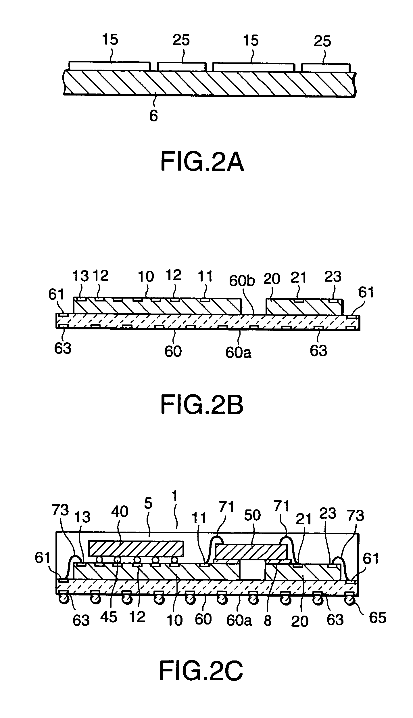
[0029]Referring to the drawings, the present invention will be described in the following.
[0030]Referring to FIG. 1, semiconductor device 1 of this embodiment includes at least, for example, two intermediate substrates 10 and 20, three IC chips 40, 50 and 52 being electronic components, and a printed wiring board (referred to as PWB hereinafter).
[0031]First, description about principal configuration of each element is in order. The IC chip 40 has pad electrodes (not shown) for external connection on its surface side with elements formed on it, and solder bumps, for example, are formed on the electrodes. The IC chips 50 and 62 have bonding pads (not shown) serving as external connection electrodes on the surface side where elements are formed. Both of the intermediate substrates 10 and 20 are formed of silicon substrate with almost square or rectangular outer shape, and have a size, for example, of a square with a side of 20 mm or less that permits batch exposure by a general reducti...
PUM
 Abstract
Description
Claims
Application Information
PatSnap Eureka turns technology decisions into work you can execute. Powered by our Innovation Knowledge Graph, it runs expert workflows across engineering, life sciences, materials and intellectual property. Get your review-ready output in minutes.


