Method and apparatus for optimized parallel testing and access of electronic circuits

a technology of parallel testing and access, applied in the field of scan-based testing of integrated circuits, printed circuit boards, systems, etc., can solve the problems of limited ate testing to a single uut, and the scalability of traditional ate is often impractical

Inactive Publication Date: 2006-01-17
INTELLITECH INC
View PDF12 Cites 173 Cited by
  • Summary
  • Abstract
  • Description
  • Claims
  • Application Information

AI Technical Summary

Benefits of technology

[0028]The presently disclosed parallel test architecture provides a low-cost optimal solution to parallel testing of electronic circuits and/or configuration of programmable circuits. It can b...

Problems solved by technology

Typically, ATE is limited to testing a single UUT or only a few devices in parallel.
Further, scalability of traditional ATE is often impractical, as ...

Method used


Image

  • Method and apparatus for optimized parallel testing and access of electronic circuits
  • Method and apparatus for optimized parallel testing and access of electronic circuits
  • Method and apparatus for optimized parallel testing and access of electronic circuits

Examples


Embodiment Construction

[0046]U.S. Provisional Patent Application No. 60 / 303,052 filed Jul. 5, 2001 is incorporated herein by reference.

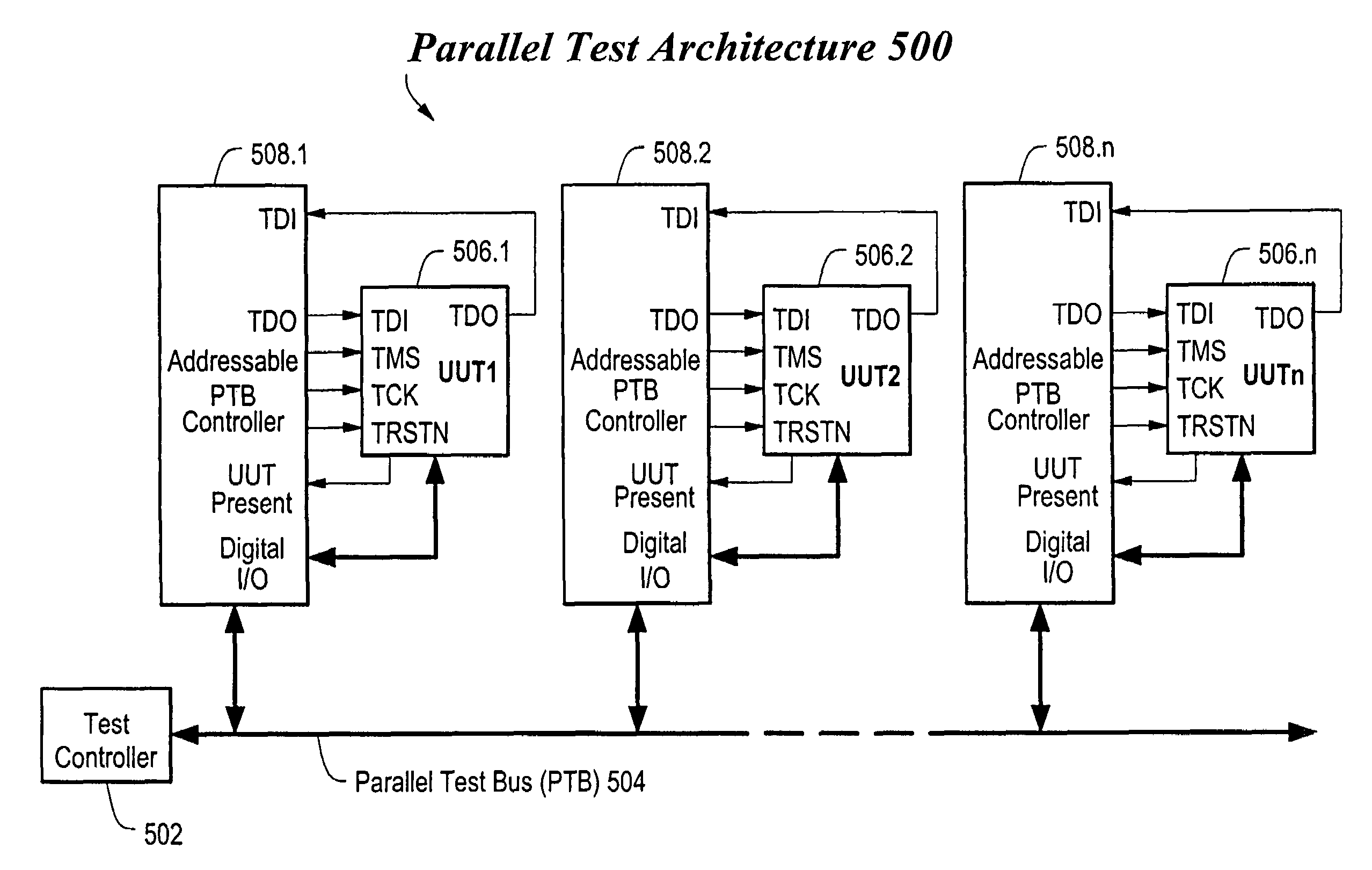
[0047]FIG. 5 depicts an illustrative embodiment of a Parallel Test Architecture (PTA) 500, in accordance with the present invention. In the illustrated embodiment, a test controller 502 is connected to a Parallel Test Bus (PTB) 504. For example, the test controller 502 may be either a separate external test controller or an embedded master controller, e.g., embedded with the system including Units Under Test (UUTs) 506.1–506.n. The test controller 502 is configured to communicate over the PTB 504 using the protocol of the PTA 500, which is described below. In this illustrated embodiment, the UUTs 506.1–506.n are connected to the PTB 504 via respective addressable PTB Controller circuits 508.1–508.n. Further, the PTA 500 may have from 1-n UUTs connected to the PTB 504. Any suitable number of like UUTs may then be accessed in parallel for testing and / or debugging purposes, o...


PUM


Abstract

An architecture that provides stimulus data and verifies the response of multiple electronic circuits substantially in parallel for optimized testing, debugging, or programmable configuration of the circuits. The architecture includes a test bus, a primary test controller connected to the bus, and a plurality of local test controllers connected to the bus, in which each local test controller is coupleable to a respective circuit. The primary test controller sends stimulus data and expected response data over the bus to the respective local test controllers to perform parallel testing, debugging or programmable configuration of the circuits. Each local test controller applies the stimulus data and verifies the circuit response against the expected response data. Further, each local test controller stores the result of the verification for later retrieval by the primary test controller.

Description

CROSS REFERENCE TO RELATED APPLICATIONS[0001]This application claims priority of U.S. Provisional Patent Application No. 60 / 303,052 filed Jul. 5, 2001 entitled METHOD AND APPARATUS FOR OPTIMIZED PARALLEL TESTING AND ACCESS OF ELECTRONIC CIRCUITS.STATEMENT REGARDING FEDERALLY SPONSORED RESEARCH OR DEVELOPMENT[0002]N / ABACKGROUND OF THE INVENTION[0003]The present invention relates generally to scan-based testing of integrated circuits, printed circuit boards, and systems, and more particularly to a method and apparatus for accessing multiple such electronic circuits within a system and for optimized testing of multiple such electronic circuits in parallel.[0004]Scan-based testing is frequently employed during the development and manufacturing of electronic components (e.g., Integrated Circuits (ICs)) and systems (e.g., Printed Circuit Boards (PCBs) and Systems On a Chip (SoC) for detecting and diagnosing defects and for debugging. This test method is commonly referred to as “scan” beca...

Claims


Application Information

Patent Timeline
IPC IPC(8): G06F11/00G01R31/28G01R31/3185G06F11/22G11C29/56
CPCG11C29/56G01R31/318563G01R31/318516G01R31/318555G11C2029/2602G01R31/28
Inventor RICCHETTI, MICHAELCLARK, CHRISTOPHER J.
Owner INTELLITECH INC
Why Eureka
Try Eureka