Projection optical system, projection type image display apparatus, and image display system
a projection optical and projection technology, applied in the direction of optical elements, television systems, instruments, etc., can solve the problems of low assemble accuracy, low accuracy of mirror arrangement, and degradation of optical performance, and achieve the effect of small tilt angle of respective reflecting surfaces and large angl
- Summary
- Abstract
- Description
- Claims
- Application Information
AI Technical Summary
Benefits of technology
Problems solved by technology
Method used
Image


Examples
embodiment 1
[0071](Embodiment 1)
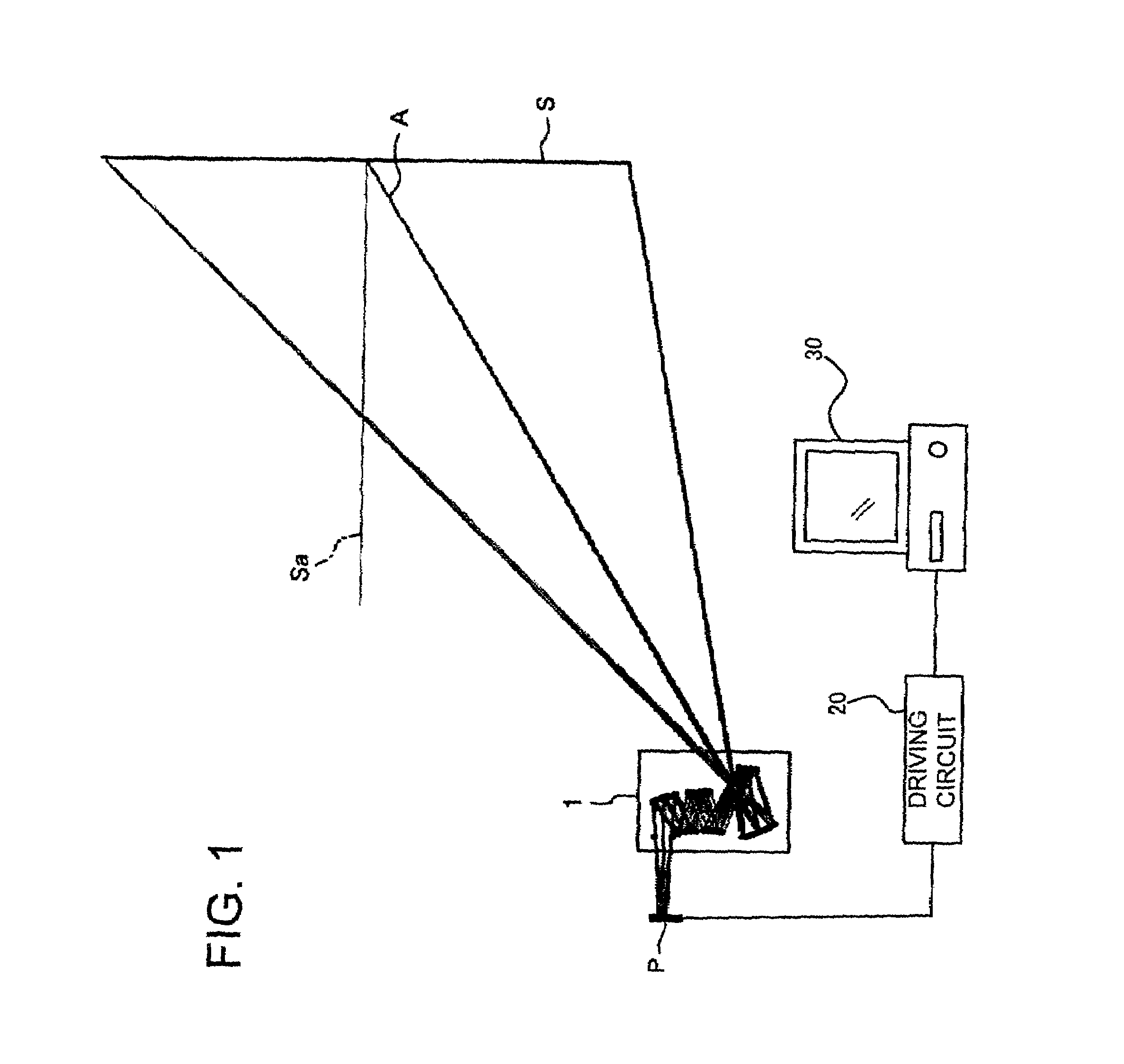
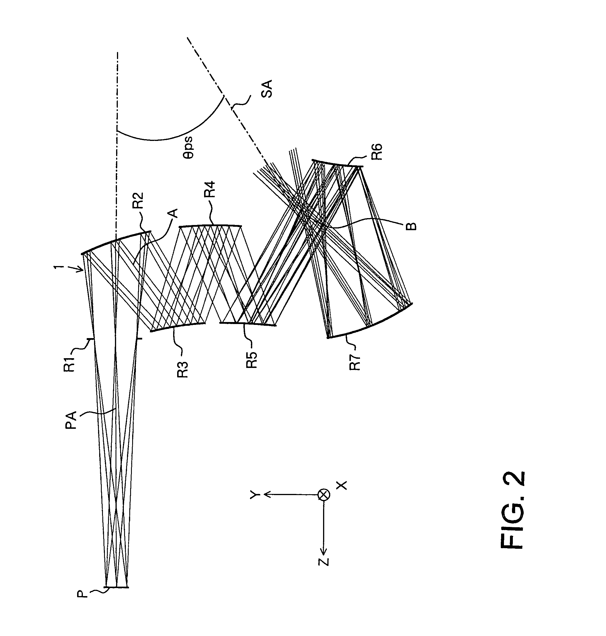
[0072]FIG. 1 shows all optical systems of a projector (a projection type image display apparatus) including a projection optical system which is Embodiment 1 of the present invention. FIG. 2 shows the structure of the projection optical system.
[0073]In FIGS. 1 and 2, P shows an image forming element for which a reflective type dot matrix liquid crystal display, a digital micromirror device (DMD), a self-light-emitting element (such as an organic electroluminescence element) or the like is used. Reference numeral 1 shows the projection optical system for enlargingly projecting an original image formed on the image forming element P onto a screen S.
[0074]A driver circuit 20 is connected to the image forming element P for driving thereof. Connected to the driving circuit 20 is an image information supply apparatus 30 such as one of various computers, a camera (a video camera, a digital camera or the like), a VCR, a cellular phone, and a radio wave receiver (wired or...
embodiment 2
[0136](Embodiment 2)
[0137]FIG. 5 shows all optical systems of a projector including a projection optical system which is Embodiment 2 of the present invention. FIG. 6 shows the structure of the projection optical system.
[0138]In FIGS. 5 and 6, P shows an image forming element for which a reflective type dot matrix liquid crystal display, a digital micromirror device (DMD), a self-light-emitting element (such as an organic electroluminescence element) or the like is used. Reference numeral 2 shows the projection optical system for enlargingly projecting an original image formed on the image forming element P onto a screen S.
[0139]In Embodiment 2, the image forming element P has a size of 17.4 mm×9.8 mm, and the screen S has a size of 60 inches diagonally with an aspect ratio of 16:9. A normal line Sa to the screen S is inclined by 36 degrees with respect to the reference axis A. The incident side reference axis PA of the projection optical system 2 forms an angle θps of 126 degrees w...
embodiment 3
[0192](Embodiment 3)
[0193]FIG. 9 shows an optical system which is Embodiment 3 of the present invention. P shows an image forming element for which a reflective type dot matrix liquid crystal display, a digital micromirror device (DMD), a self-light-emitting element (such as an organic electroluminescence element) or the like is used. It goes without saying that a transmissive type image forming element may be used.
[0194]The image forming element P is inclined by 10 degrees with respect to the reference axis A. Reference numeral 3 shows a projection optical system for enlargingly projecting an original image formed on the image forming element P onto a screen S. FIG. 10 shows the projection optical system 3 in detail.
[0195]The image forming element P has a size of 17.4 mm×9.8 mm, and the screen S has a size of 60 inches diagonally with an aspect ratio of 16:9. A normal line Sa to the screen S is inclined by 42.53 degrees with respect to the reference axis A. The incident side refere...
PUM
 Abstract
Description
Claims
Application Information
 - R&D
- Intellectual Property
- Life Sciences
- Materials
- Tech Scout
- Unparalleled Data Quality
- Higher Quality Content
- 60% Fewer Hallucinations
Browse by: Latest US Patents, China's latest patents, Technical Efficacy Thesaurus, Application Domain, Technology Topic, Popular Technical Reports.
© 2025 PatSnap. All rights reserved.Legal|Privacy policy|Modern Slavery Act Transparency Statement|Sitemap|About US| Contact US: help@patsnap.com