
Eureka
For R&D, Eureka makes reading and utilizing patents & technical documents easy.
Eureka AIR
Designed for self-driven R&D workflows. Generate viable solutions, solve complex R&D challenges, empower your innovation with AI.

Eureka Materials
Designed for material experts only. Revolutionize your material R&D, from search, analyze, to developing new materials.

TechResearch
Generate reliable direction feasibility study reports for your R&D in just a few steps.

TechSeek
Discover and master advanced knowledge NOW. Basics, ideas, possibilities, all at once.

TechMind
As an expert in R&D Theories, TechMind can generates customized viable solutions instantly.

TechRisk
Analyze your overall solution with one click, know your potential R&D risks in advance.

TechMonitor
Get weekly tech updates, stay abreast of the latest tech innovations and key insights.
Method of fabricating trench isolation structure of a semiconductor device
- Summary
- Abstract
- Description
- Claims
- Application Information
AI Technical Summary
Benefits of technology
Problems solved by technology
Method used
Image

Examples
Embodiment Construction
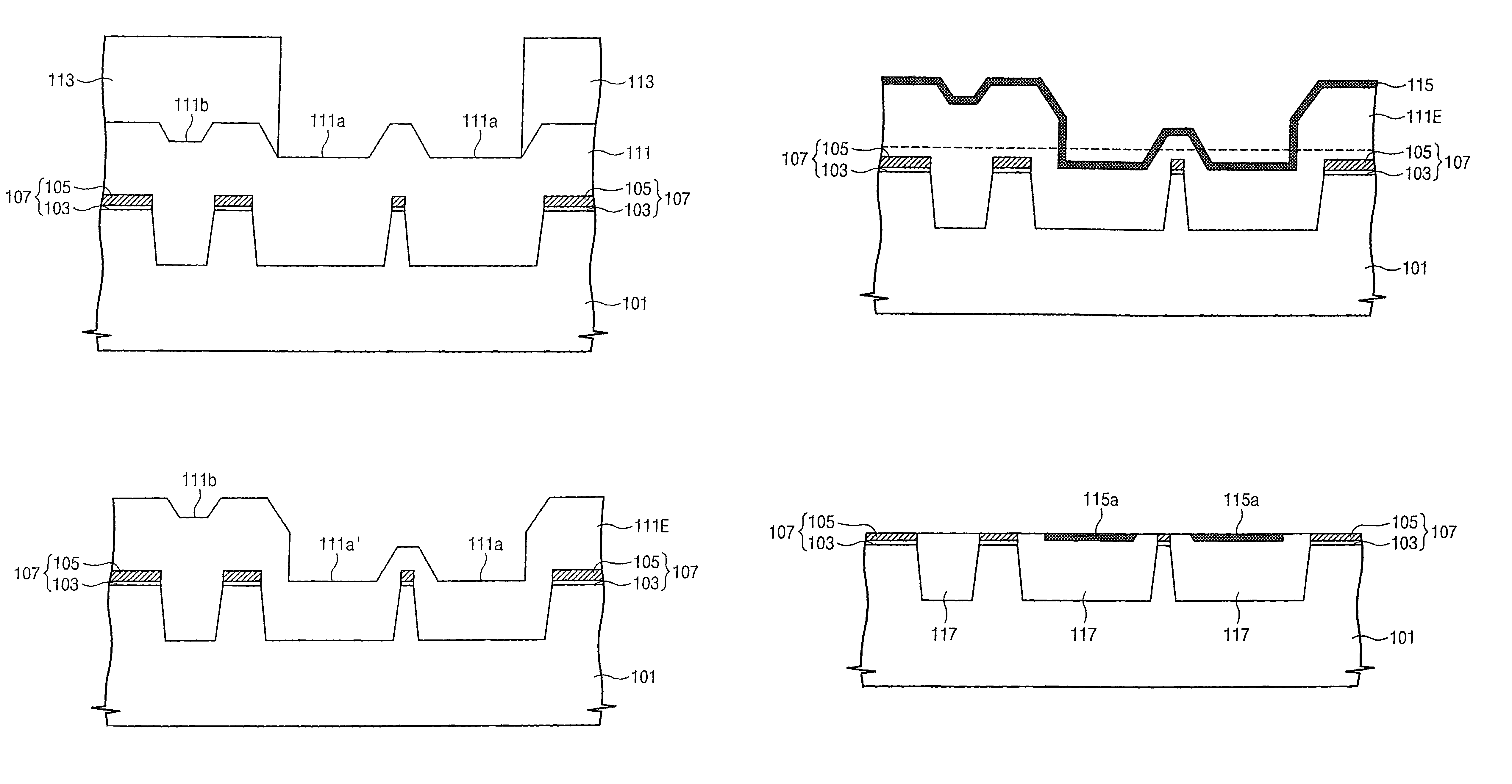
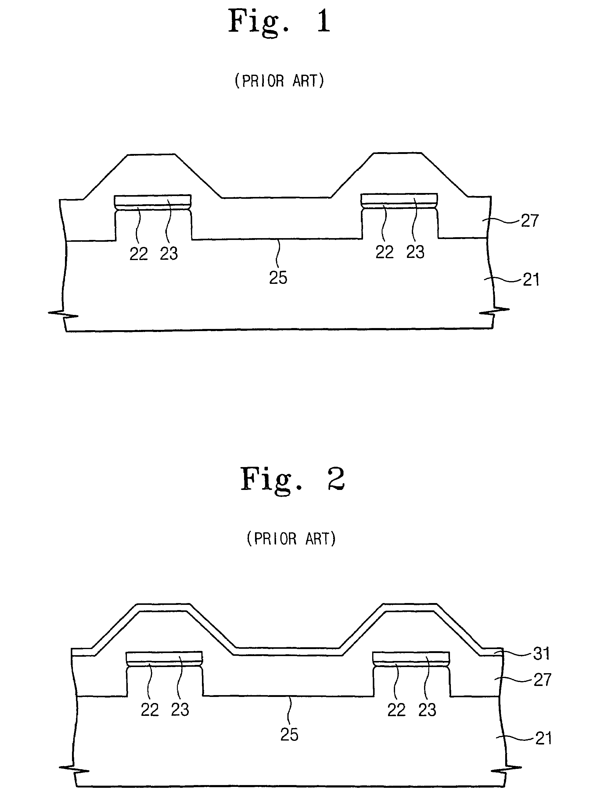
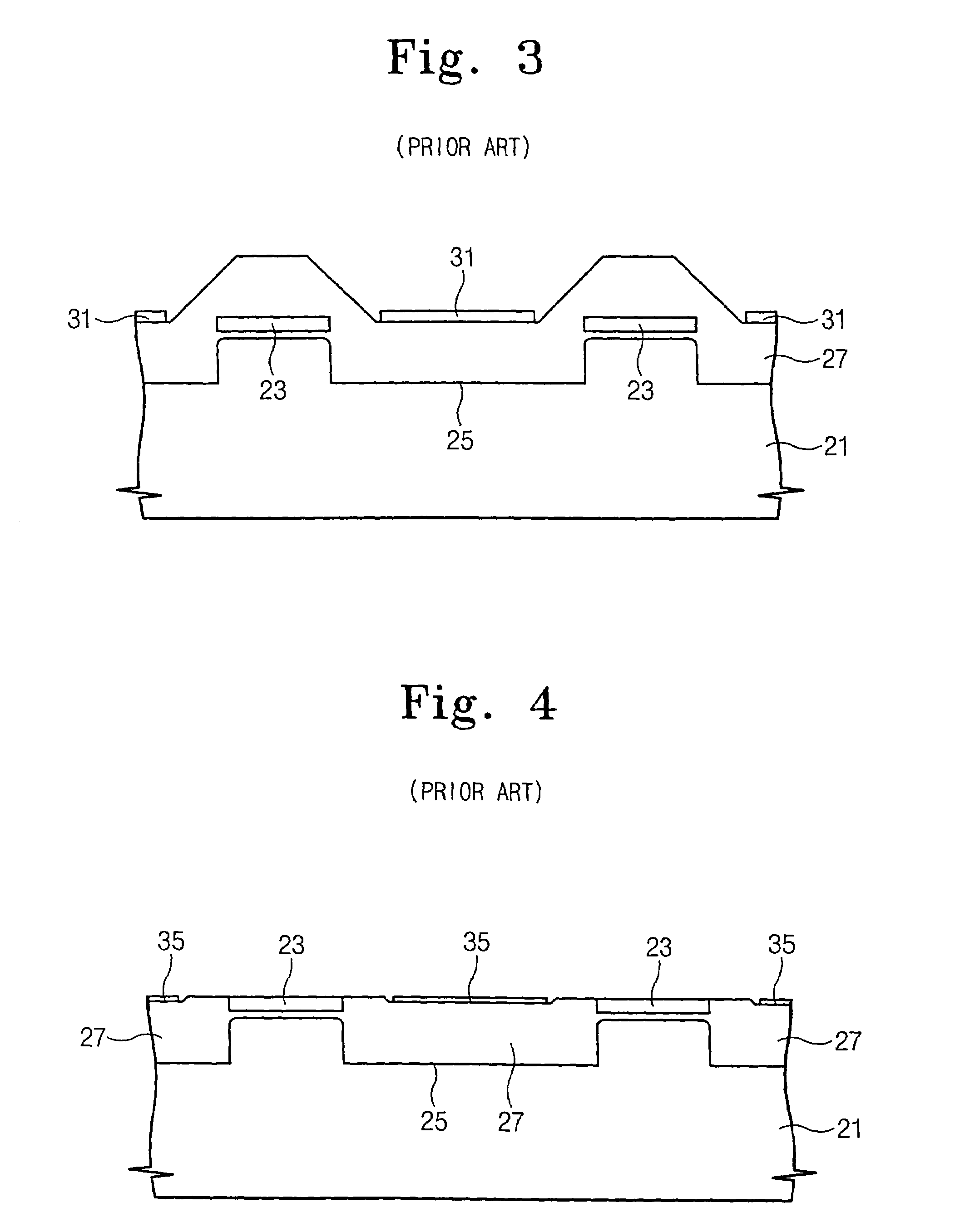
[0034]The present invention will now be described more fully hereinafter with reference to the accompanying drawings. In the drawings, the thickness of layers and regions are exaggerated for clarity. It will also be understood that when a layer is referred to as being “on” another layer or substrate, such a description refers to the referenced layer being disposed directly on the other layer or substrate, as well as additional layer(s) being interposed therebetween. Also, like reference numbers designate like elements throughout the drawings.
[0035]Referring now to FIG. 10, a trench etch mask pattern 107 is formed on a semiconductor substrate 101 to define an active region on the semiconductor substrate 101. More particularly, the portion of the semiconductor substrate 101 covered by the trench etch mask pattern 107 constitutes an active region and the portion of the semiconductor substrate exposed by the trench etch mask pattern 107 constitutes a device isolation region. The mask pa...
PUM
 Abstract
Description
Claims
Application Information
 - R&D Engineer
- R&D Manager
- IP Professional
- Industry Leading Data Capabilities
- Powerful AI technology
- Patent DNA Extraction
Browse by: Latest US Patents, China's latest patents, Technical Efficacy Thesaurus, Application Domain, Technology Topic, Popular Technical Reports.
© 2024 PatSnap. All rights reserved.Legal|Privacy policy|Modern Slavery Act Transparency Statement|Sitemap|About US| Contact US: help@patsnap.com