Single semiconductor graphics platform system and method with skinning, swizzling and masking capabilities

a graphics platform and semiconductor technology, applied in the field of single semiconductor graphics platform system, can solve the problems of limited real-time display of three-dimensional objects, computational intensive process of large computation requirements for realistically rendering and displaying three-dimensional objects

Inactive Publication Date: 2006-01-31
NVIDIA CORP
View PDF18 Cites 75 Cited by
  • Summary
  • Abstract
  • Description
  • Claims
  • Application Information

AI Technical Summary

Problems solved by technology

The amount of computations needed to realistically render and display a three-dimensional graphical object, however, remains quite large and true realistic display of three-dimensional objects have largely been limited to high end systems.
Thus the process of rendering and displaying a three-dimensional object can be computationally intensive and may involve a large number of vertices.
Integration if often limited, however, by a cost of implementing and manufacturing multiple processing modules on a single chip.
In the realm of graphics processing, any attempt to integrate the transform, lighting, and rasterization modules for inc

Method used


Image

  • Single semiconductor graphics platform system and method with skinning, swizzling and masking capabilities
  • Single semiconductor graphics platform system and method with skinning, swizzling and masking capabilities
  • Single semiconductor graphics platform system and method with skinning, swizzling and masking capabilities

Examples


Embodiment Construction

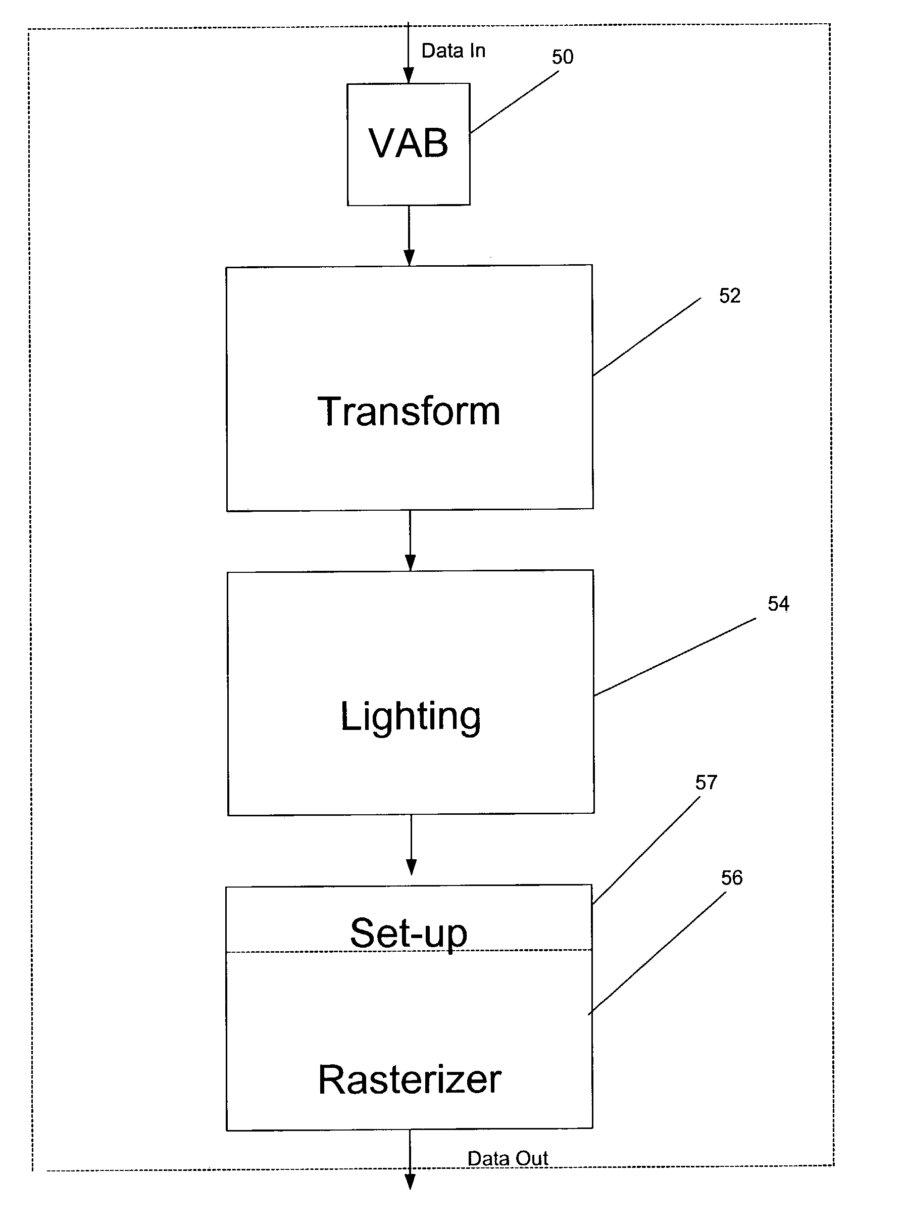
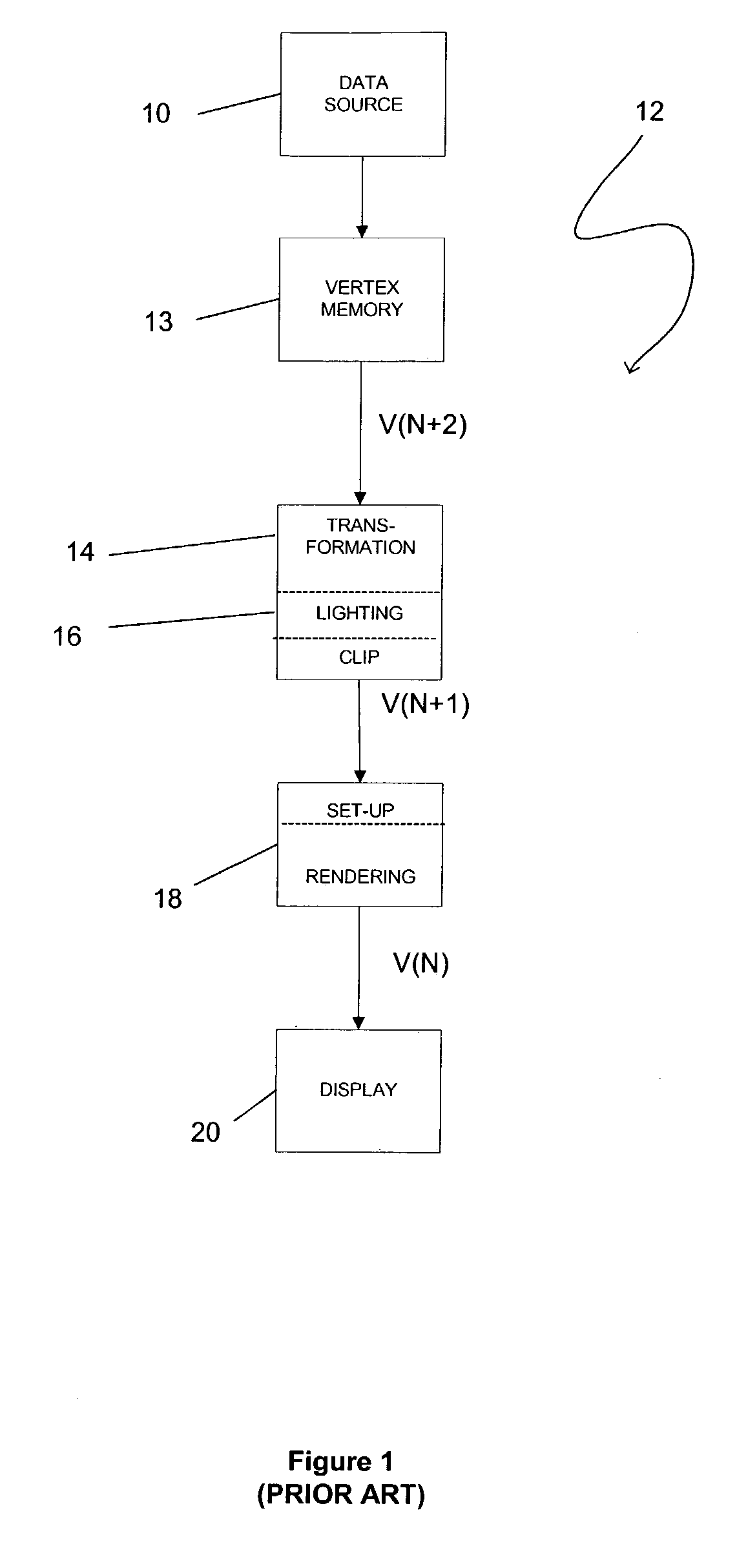
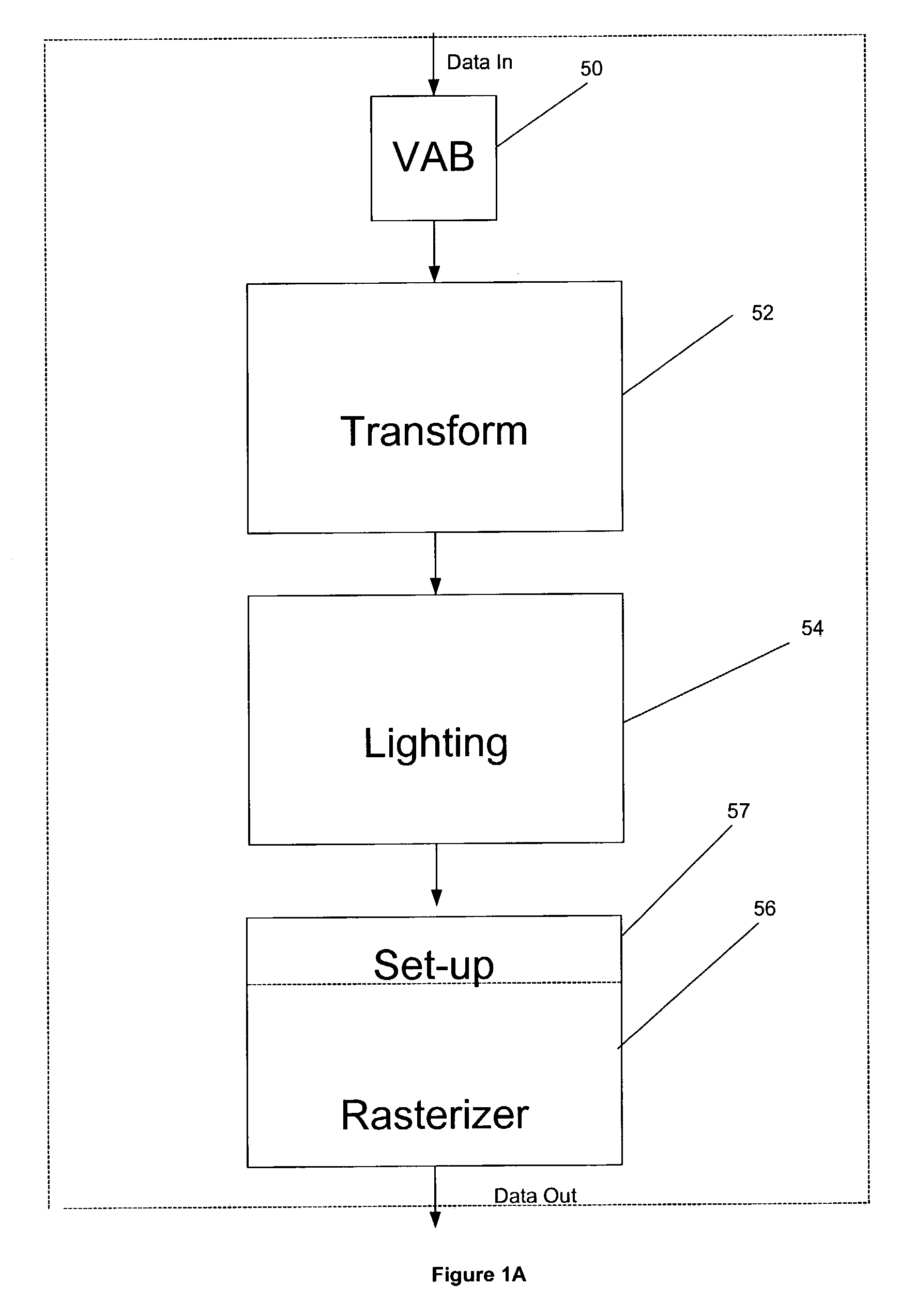
[0070]FIG. 1 shows the prior art. FIGS. 1A–32C show a graphics pipeline system of the present invention.

[0071]FIG. 1A is a flow diagram illustrating the various components of one embodiment of the present invention. As shown, the present invention is divided into four main modules including a vertex attribute buffer (VAB) 50, a transform module 52, a lighting module 54, and a rasterization module 56 with a set-up module 57. In one embodiment, each of the foregoing modules is situated on a single semiconductor platform in a manner that will be described hereinafter in greater detail. In the present description, the single semiconductor platform may refer to a sole unitary semiconductor-based integrated circuit or chip.

[0072]The VAB 50 is included for gathering and maintaining a plurality of vertex attribute states such as position, normal, colors, texture coordinates, etc. Completed vertices are processed by the transform module 52 and then sent to the lighting module 54. The transfo...


PUM


Abstract

A graphics hardware system and method are provided for graphics processing. Such system includes a transform module positioned on a single semiconductor platform for transforming graphics data. Coupled to the transform module is a lighting module which is positioned on the single semiconductor platform for lighting the graphics data. Also included is a rasterizer coupled to the lighting module and positioned on the single semiconductor platform for rendering the graphics data. As an option, the graphics hardware system may further be equipped with skinning, swizzling and masking capabilities.

Description

RELATED APPLICATIONS[0001]The present application is a continuation of an application filed Sep. 20, 2001 under Ser. No. 09 / 960,004; which, in turn, is a continuation of an application filed Dec. 5, 2000 under Ser. No. 09 / 730,652 and issued under U.S. Pat. No. 6,342,888; which, in turn, is a continuation of an application filed on Dec. 06, 1999 under Ser. No. 09 / 454,516 and issued under U.S. Pat. No. 6,198,488; which are all incorporated herein by reference in their entirety for all purposes. The present application is related to applications filed on Dec. 6, 1999 under Ser. Nos. 09 / 455,305, 09 / 454,505 which issued as U.S. Pat. No.: 6,504,542, Ser. Nos. 09 / 455,728, 09 / 454,525, 09 / 456,102 which issued as U.S. Pat. No.: 6,515,671, Ser. No. 09 / 454,524 which issued as U.S. Pat. No.: 6,353,439, and Ser. No. 09 / 456,104 which issued as U.S. Pat. No.: 6,417,851; applications filed Sep. 20, 2001 under Ser. Nos. 09 / 961,228, 09 / 961,219, and 09 / 957,746 which issued as U.S. Pat. No.: 6,462,737; ...

Claims


Application Information

Patent Timeline
IPC IPC(8): G06T17/00G06T11/40G06T15/00G06T15/04G06T15/50G09G5/37
CPCG06T11/40G06T15/005G06T15/506G06T15/50G06T15/503G06T15/04
Inventor LINDHOLM, JOHN ERIKMOY, SIMONDAWALLU, KEVINYANG, MINGJIANMONTRYM, JOHNKIRK, DAVID B.SABELLA, PAOLO E.PAPAKIPOS, MATTHEW N.VOORHIES, DOUGLAS A.FOSKETT, NICHOLAS J.
Owner NVIDIA CORP
Why Eureka
Try Eureka