Generating mask patterns for alternating phase-shift mask lithography

a phase shift mask and pattern technology, applied in the field of photolithographic methods, can solve the problems of increasing complexity of resolution enhancement techniques, increasing difficulty in lithographic patterning, and one of the fundamental limitations of high-na lithography, and the rapid loss of dof in relation to na

Inactive Publication Date: 2006-01-31
GLOBALFOUNDRIES INC
View PDF21 Cites 313 Cited by
  • Summary
  • Abstract
  • Description
  • Claims
  • Application Information

AI Technical Summary

Problems solved by technology

However, the resolution demands of the integrated circuit (IC) industry have outpaced the introduction of more advanced lithography hardware solutions for many technology generations, making lithographic patterning increasingly difficult and requiring the use of increasingly complex resolution enhancement techniques (RET) to maintain adequate pattern fidelity.
This rapid loss of DOF in relation to NA is one of the fundamental limitations of high-NA lithography.
As the drive to develop new exposure tools at shorter wavelengths continues, severe physical barriers to implementation arise in: insufficient light intensity requiring super-sensitive chemically amplified resist systems, increased light absorption forcing more exotic optical materials and tighter cleanliness specifications on all optical components including the photomask, and ultimately, the need to operate in vacuum with reflective optics.
Controlling critical parameters such as aberrations and focal plane flatness over large areas during lens manufacturing has made the introduction of NAs larger than 0.7 very difficult.
However, k1 has been continuously declining in spite of tooling improvements; i.e., lithography has been losing ground due to ever harder technology generations.
Violation of this rule results in a residual resist image on the wafer, or, in other words, unexposed resist that can cause defects on the wafer.
While block masks and phase masks must each conform to their own set of unique manufacturability and lithography constraints, problems arise when the block mask is legalized independently from the phase-shifting mask, or vice versa.
A problem with the prior art method of FIG. 4 is the need to continually modify the layout by going back to the redefinition of critical segments.
While the optimization altPSM parameters as provided above show great promise in improving lithographic performance, the circular definition of mask features challenges the capabilities of current tools to generate suitable altPSM and block mask combinations.
However, there is yet much to do before the shapes of both masks are finalized.
However, the actual layouts of different chips present many complicated topologies in which predicting the geometry of the block mask shapes is difficult to do accurately based on the phase patterns to be generated.

Method used


Image

  • Generating mask patterns for alternating phase-shift mask lithography
  • Generating mask patterns for alternating phase-shift mask lithography
  • Generating mask patterns for alternating phase-shift mask lithography

Examples


Embodiment Construction

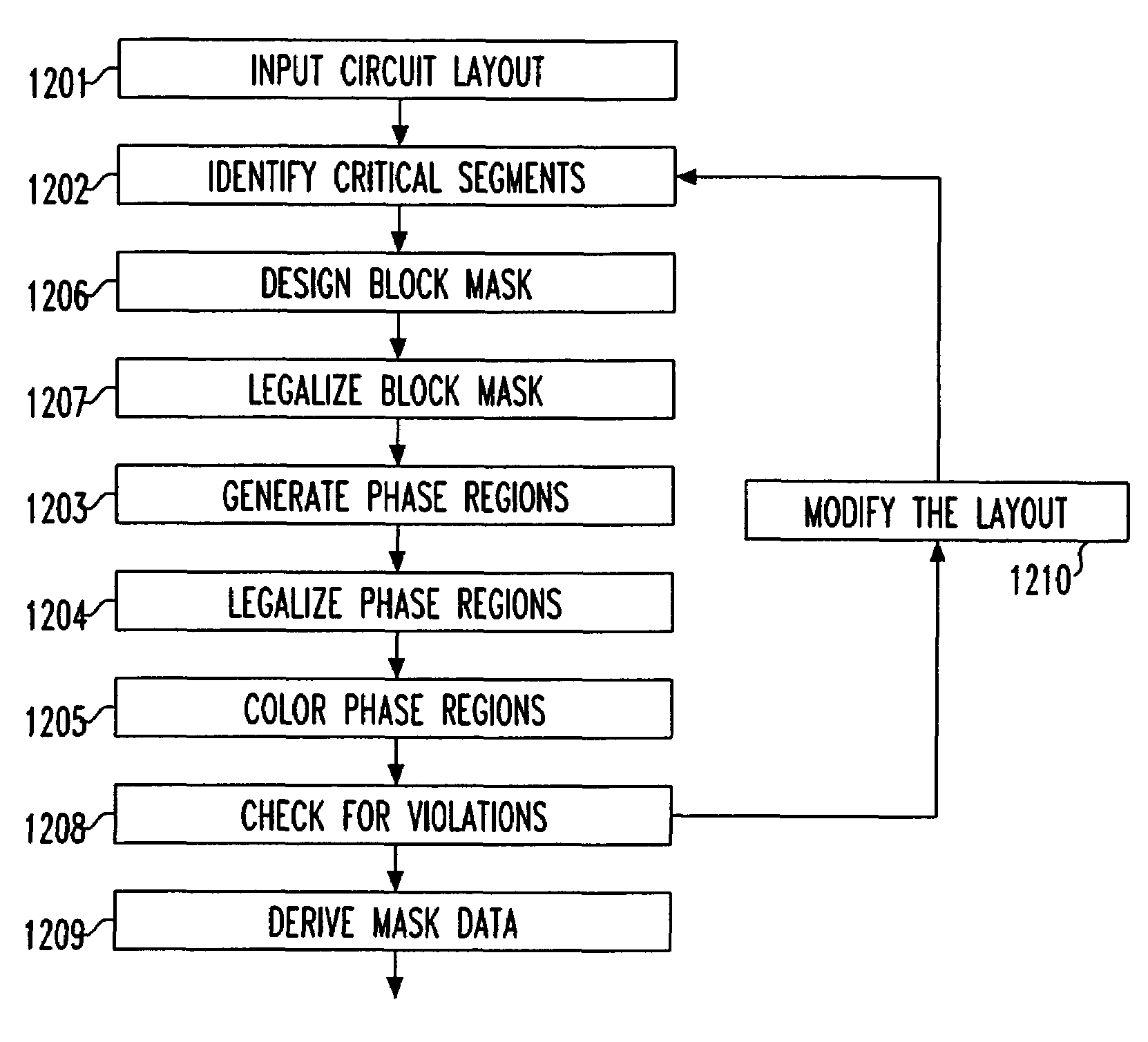
[0064]FIG. 12 is a flowchart illustrating an embodiment of the present invention. As indicated above, it is desirable to improve the process and flow for generating the patterns of a pair of an alternating phase-shifting mask (altPSM) and block (trim) mask used together in a dual exposure lithography method. It is desirable to generate pairs of altPSM and trim masks from input circuit layout data in a way that lithographically optimized and logically correct exposure patterns can be produced on a wafer. In furtherance of these goals, and towards reducing the time and processor resources required to generate patterns for such mask pairs, in an embodiment of the invention, an approach is provided for defining all parameters of the block (trim) mask only as a function of the primary circuit layout. Thereafter, parameters of the phase shape patterns are defined as a function of both the primary circuit layout, as well as the block mask patterns.

[0065]In the embodiment shown in FIG. 12, ...


PUM

PropertyMeasurementUnit
half wavelengthsaaaaaaaaaa
wavelengthaaaaaaaaaa
diffracted angleaaaaaaaaaa

Abstract

A method of generating patterns of a pair of photomasks from a data set defining a circuit layout to be provided on a substrate includes identifying critical segments of the circuit layout to be provided on the substrate. Block mask patterns are generated and then legalized based on the identified critical segments. Thereafter, phase mask patterns are generated, legalized and colored. The legalized block mask patterns and the legalized phase mask patterns that have been colored define features of a block mask and an alternating phase shift mask, respectively, for use in a dual exposure method for patterning features in a resist layer of a substrate.

Description

BACKGROUND OF INVENTION[0001]This invention relates to photolithographic methods employed in the manufacture of very large-scale integrated (VLSI) circuits and more specifically to improved methods for generating patterns of photomasks.[0002]Optical lithography has long been a key enabler to the rapid pace of integration that fuels the microelectronics industry. However, the resolution demands of the integrated circuit (IC) industry have outpaced the introduction of more advanced lithography hardware solutions for many technology generations, making lithographic patterning increasingly difficult and requiring the use of increasingly complex resolution enhancement techniques (RET) to maintain adequate pattern fidelity.[0003]To put the discussion on RET and their impact on layout into proper context, it will be helpful to first review some simplified concepts of optical lithography, and then review the exposure tool options for the next two major sub-90 nm technology nodes, and then d...

Claims


Application Information

Patent Timeline
Patent Type & Authority Patents(United States)
IPC IPC(8): G06F17/50G03C1/00G03F5/00G03F1/08G03C3/02G03C5/00G03F1/00G03F9/00H01L21/027
CPCG03F1/30G03F1/70
Inventor LIEBMANN, LARS W.BUKOFSKY, SCOTT J.GRAUR, IOANA
Owner GLOBALFOUNDRIES INC
Why Eureka
Try Eureka