Active wafer cooling during damage engineering implant to enhance buried oxide formation in SIMOX wafers

a technology of active wafers and engineering implants, which is applied in the direction of semiconductor devices, electrical equipment, basic electric elements, etc., can solve the problems of limited degree of cooling that such approaches afford

Inactive Publication Date: 2006-02-14
IBIS TECH
View PDF23 Cites 13 Cited by
  • Summary
  • Abstract
  • Description
  • Claims
  • Application Information

AI Technical Summary

Benefits of technology

[0015]In another aspect, each of the first and second chambers includes an apparatus for generating ions with energies in a selected range, e.g., 30 to 500 keV, and for directing the ions onto the substrate surface, to effect implantation of the ions at a selected depth below the substrate surface.

Problems solved by technology

A major disadvantage of such passive cooling has been the limited degree of cooling that such approaches afford.

Method used


Image

  • Active wafer cooling during damage engineering implant to enhance buried oxide formation in SIMOX wafers
  • Active wafer cooling during damage engineering implant to enhance buried oxide formation in SIMOX wafers
  • Active wafer cooling during damage engineering implant to enhance buried oxide formation in SIMOX wafers

Examples


Embodiment Construction

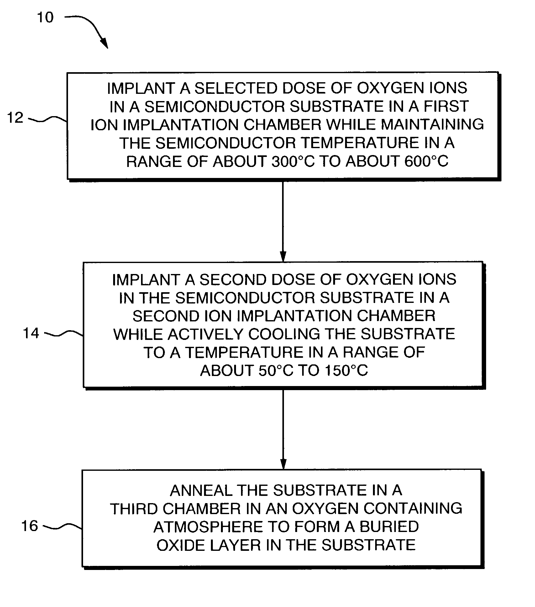
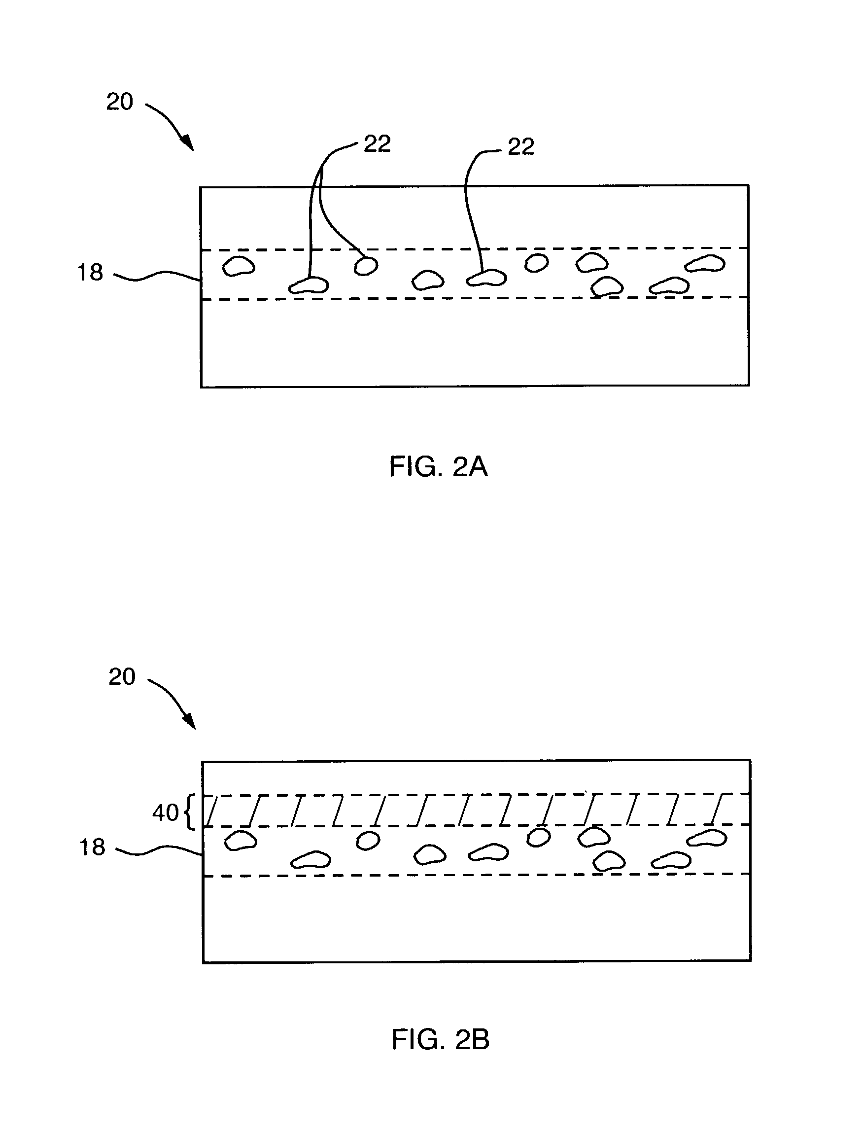
[0027]The present invention provides methods and systems for forming a buried oxide (BOX) region in a semiconductor substrate, such as, silicon, by implanting oxygen ions in the substrate in at least two distinct steps, performed at two different temperature regimes, followed by an annealing step at an elevated temperature in an oxygen containing atmosphere. In the first implantation step, a dose of oxygen ions in a range of about 1016 to about 1018 ions / cm2 is implanted in the substrate. In the second implantation step, another dose of oxygen ions, for example, in a range of about 1013 to about 5×10¹⁵ ions / cm2, is implanted in the substrate while the substrate temperature is actively maintained in a range of approximately 50 to 150° C. Subsequently, an annealing step in an oxygen-containing atmosphere is performed to generate a continuous BOX region.

[0028]Although in the exemplary embodiments described below the semiconductor substrate is selected to be silicon, a method according ...


PUM


Abstract

The present invention provides methods and system for forming a buried oxide layer (BOX) region in a semiconductor substrate, such as, a silicon wafer. In one aspect, in a method of the invention, an initial dose of oxygen ions is implanted in the substrate while maintaining the substrate temperature in a range of about 300° C. to 600° C. Subsequently, a second dose of oxygen ions is implanted in the substrate while actively cooling the substrate to maintain the substrate temperature in range of about 50° C. to 150° C. These ion implantation steps are followed by an annealing step in an oxygen containing atmosphere to form a continuous BOX region in the substrate. In one preferred embodiment, the initial ion implantation step is performed in a chamber that includes a device for heating the substrate while the second ion implantation step is performed in a separate chamber that is equipped with a device for actively cooling the substrate. The annealing step can be performed in a third chamber or in either of the first or second chambers.

Description

BACKGROUND OF THE INVENTION[0001]The present invention relates generally to methods and systems for generating a buried insulating layer in a semiconductor substrate. More particularly, the invention provides methods and systems for forming a buried oxide layer in a semiconductor substrate, such as, silicon.[0002]One method known in the art as Separation by Implantation of Oxygen (SIMOX) forms a thin buried oxide (BOX) layer in a semiconductor substrate, such as silicon, by bombarding the substrate with energetic oxygen ions at a high dose. Typically, the substrate is heated to a temperature of about 400° C. to 600° C. during this implantation so that damage to crystal structure of the substrate is offset, in part, by “self-annealing.”Following implantation, residual damage in the substrate is removed and buried oxide layer is formed by a further annealing step at an elevated temperature of about 800° C. or higher. The buried oxide layer can function as an insulating layer that sepa...

Claims


Application Information

Patent Timeline
Patent Type & Authority Patents(United States)
IPC IPC(8): H01L21/31H01L21/265H01L21/02H01L21/762H01L27/12
CPCH01L21/76243Y10S438/966
Inventor EROKHIN, YURIBLAKE, JULIAN G.
Owner IBIS TECH
Why Eureka
Try Eureka