Electrostatic discharge protection device with complementary dual drain implant

a protection device and dual-drain technology, applied in the direction of semiconductor devices, semiconductor/solid-state device details, electrical apparatus, etc., can solve the problems of gate oxide damage, multi-finger turn-on is very difficult, and the issue of multifinger turn-on, etc., to increase the junction radius, enhance the electric field, and increase the surface area for breakdown

Active Publication Date: 2006-02-14
CHARTERED SEMICONDUCTOR MANUFACTURING +1
View PDF9 Cites 10 Cited by
  • Summary
  • Abstract
  • Description
  • Claims
  • Application Information

AI Technical Summary

Benefits of technology

[0012]It is an object of at least one embodiment of the present invention to provide a method and a device to improve the ESD protection of off-chip driver (OCD) NMOS transistors.
[0014]It is yet another object of the present invention to reduce the breakdown voltage of the drain / substrate junction during an ESD event.
[0015]It is still another object of the present invention to increase the junction area which participates in the avalanche breakdown.
[0017]These and many other objects have been achieved by an additional P-ESD implant between the N-well implant and the N+ drain region of the OCD NMOS transistor. The P-ESD implant will be dosed less than the N+ source / drain implants but higher than the N-well dose. In another embodiment of the invention, N-well doping is used in conjunction with the P-ESD doping, where the P-ESD doping is chosen such that it counterdopes the N-well underneath the N+ drain. P-ESD doping is done in such a way that the N-well underneath still maintains electrical connection to N+ drains over it. The P-ESD region is also electrically connected to the P+ substrate. This procedure creates a larger surface under the area where the junction breakdown occurs and an increased radius of curvature of the junction, and results in an enhanced electric field and a breakdown at lower voltage during an ESD event. The P-ESD implants are covered by N-type on three sides which creates more surface area for breakdown and better parasitic bipolar transistor characteristics. The total junction area for breakdown can be further increased by increasing the perimeter surface of the P-ESD implant.

Problems solved by technology

Unfortunately, such a solution does nothing to decrease the avalanche voltage (Vt1) of the transistor, thus making multifinger turn-on very difficult, as illustrated in FIG. 1b where the current ITLP is graphed against the voltage VTLP.
As a result, Vt2 (second breakdown voltage) of the ESD device is oftentimes lower than Vt1, resulting in the issue of multifinger turn-on.
Furthermore, it is known that Vt1 is generally higher than the gate oxide breakdown voltage for submicron MOSFETSs and if nothing is done to reduce it will cause gate oxide damage even during the brief time for the transistor to turn on.
Additionally, even if the gate oxide is not damaged it will cause significant hot carrier degradation, resulting in poor drive of the OCD as time goes on.

Method used


Image

  • Electrostatic discharge protection device with complementary dual drain implant
  • Electrostatic discharge protection device with complementary dual drain implant
  • Electrostatic discharge protection device with complementary dual drain implant

Examples


Embodiment Construction

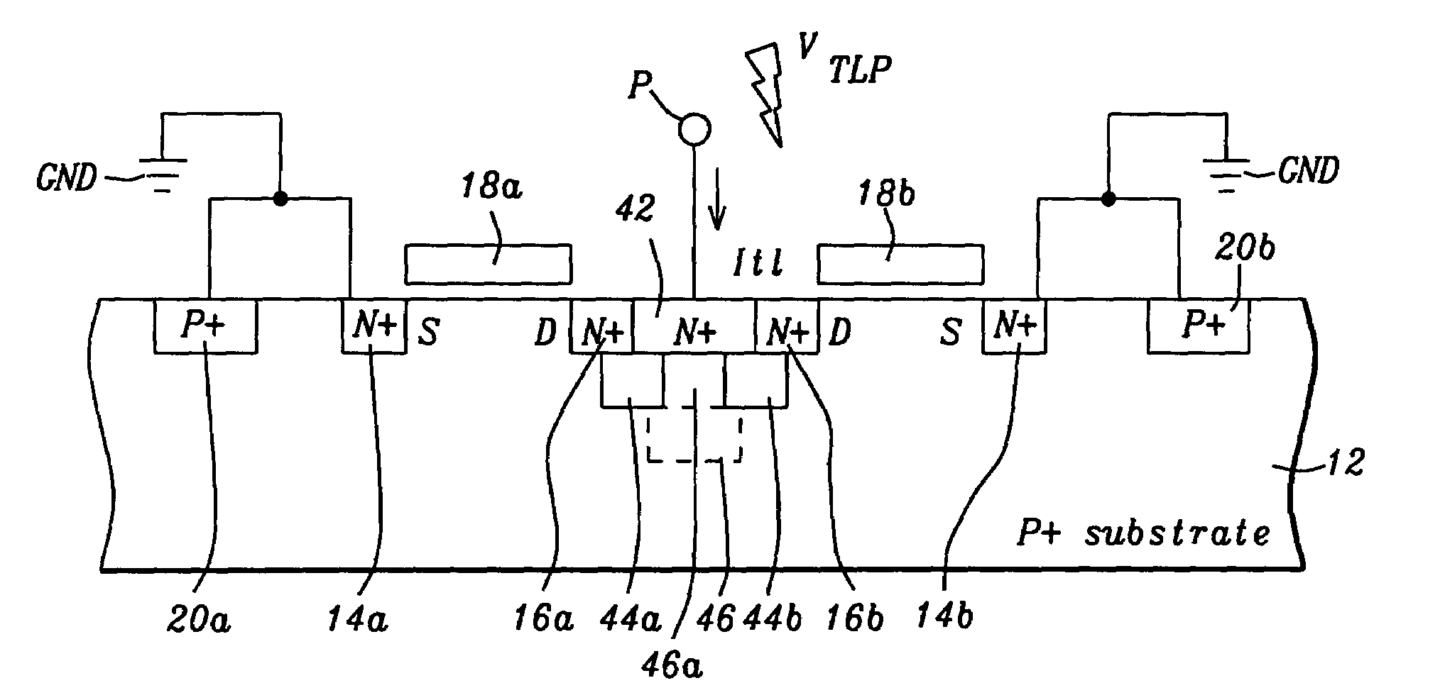
[0037]Referring now to the accompanying drawings FIGS. 4a–d, and FIGS. 5b–d, there are shown embodiments of the invention. FIG. 4a is a first preferred embodiment of the invention and differs from FIG. 1a by having NMOS OCD A and NMOS OCD B arranged in a mirror symmetry around a vertical line through Point P. Like in FIG. 1a, an ESD pulse VTLP is applied at point P. The device described in this invention lowers the Vt1 of the transistor by implementing additional P-ESD implants 44a, 44b and N-well implants 46, 46a below the N+ drain regions 16a, 16b of the N+ junction 42. The device can be implemented in a first and a second preferred embodiment. In the first preferred embodiment, P-ESD implants 44a, 44b are used underneath drains 16a, 16b, respectively. This arrangement will reduce the breakdown voltage of the drain / substrate (16a / 12, 16b / 12) junction. The P-ESD implant dose should be less than the N+ source / drain conditions, but higher than the N-well 46, 46a dose for the process....


PUM


Abstract

Off-chip driver (OCD) NMOS transistors with ESD protection are formed by interposing an P-ESD implant between the N+ drain regions of OCD NMOS transistors and the N-well such that the P-ESD surrounds a section of the N-well. The P-ESD implant is dosed less than the N+ source / drain implants but higher than the N-well dose. In another embodiment, N-well doping is used along with P-ESD doping, where the P-ESD doping is chosen such that it counterdopes the N-well underneath the N+ drains. The N-well, however, still maintains electrical connection to the N+ drains. This procedure creates a larger surface under the area where the junction breakdown occurs and an increased radius of curvature of the junction. The P-ESD implant is covered by N-type on three sides creating better parasitic bipolar transistor characteristics.

Description

BACKGROUND OF THE INVENTION[0001]1. Field of the Invention[0002]The invention relates to the protection of integrated circuits from electrostatic discharge (ESD), and more particularly to structures for the to protection from ESD by adding P-ESD implants and an additional N-well to the drains of an off-chip driver (OCD) NMOS transistor.[0003]2. Description of the Related Art[0004]The protection of integrated circuits from electrostatic discharge (ESD) has received a lot of attention. Many researchers in this field have proposed solutions to protect submicron devices without requiring any increase of silicon real estate. FIG. 1a depicts a cross-section of the related art showing in a P+ substrate 12 an OCD NMOS transistor A with N+ source 14a, drain 16a, a gate 18a, and a P+ type diffusion 20a. The source 14a, the gate 18a, and P+ substrate 12 (via P+ type diffusion 20a) are shown tied to ground (GND). An ESD pulse VTLP at point P is shown discharging into drain 16a with current ITLP...

Claims


Application Information

Patent Timeline
Patent Type & Authority Patents(United States)
IPC IPC(8): H01L23/62H01L27/02H01L29/08H01L29/10H01L29/78
CPCH01L27/0266H01L29/0847H01L29/1083H01L29/78H01L2924/0002H01L2924/00
Inventor MANNA, INDRAJITLO, KENG FOOTAN, PEE YACHENG, MICHAEL
Owner CHARTERED SEMICONDUCTOR MANUFACTURING
Why Eureka
Try Eureka