Method for limiting slip lines in a semiconductor substrate

a technology of semiconductor substrates and slip lines, which is applied in the direction of semiconductor/solid-state device manufacturing, basic electric elements, electric devices, etc., can solve the problems of increasing production capacity, limiting the negative effect of polishing, and undesirable slip lines in the treated wafers, so as to reduce the generation of slip lines

Active Publication Date: 2006-02-21
SOITEC SA
View PDF12 Cites 2 Cited by
  • Summary
  • Abstract
  • Description
  • Claims
  • Application Information

AI Technical Summary

Benefits of technology

[0008]The present invention relates to a method for limiting slip lines in a semiconductor substrate that includes a support layer and a useful semiconductor layer that is transferred to the support layer. The technique includes precipitating at least a portion of interstitial oxygen in the support layer by a series of heat treatments conducted after bonding of the useful semiconductor layer to the support layer, at a temperature and a time sufficient to reduce the generation of slip lines therein.
[0009]In an advantageous embodiment, the semiconductor substrate is fabricated by implanting species through a surface of a source substrate to form a zone of weakness, bonding the surface of the source substrate to a support layer having an initial quantity of interstitial oxygen, detaching the useful layer from the source substrate along the zone of weakness to form the semiconductor substrate, and finishing the semiconductor substrate. At least one of the heat treatments may advantageously occur during detachment of the useful layer from a source substrate, or during a thermal oxidation or deoxidation step that occurs during a finishing step of the semiconductor substrate, or during a heat treatment to strengthen a bonding interface between the useful layer and the support layer. In this manner the same equipment normally used for heat treatments during the fabrication process can be used to precipitate interstitial oxygen, any wafer adjustments are minimized, time is saved, and productivity is improved. The predetermined limit of slip lines may be expressed as the number of slip lines per unit surface area.

Problems solved by technology

The polishing time necessary to obtain a satisfactory roughness value is thus reduced or even avoided, thus increasing production capacity and also limiting the negative effects of polishing, in particular as regards uniformity in the thickness of the thin layer.
However, heat treatments, and in particular rapid thermal annealing (RTA) treatments, include rapid temperature rises and very high temperatures (typically 1200° C. in less than one minute).
Such finishing treatments are necessary for the production of an SOI substrate wafer but also tend to cause undesirable slip lines in the treated wafer.
Further, slip lines weaken the substrate and can lead to rupture of the structure during subsequent heat treatment(s) that are used to produce the components.

Method used


Image

  • Method for limiting slip lines in a semiconductor substrate
  • Method for limiting slip lines in a semiconductor substrate
  • Method for limiting slip lines in a semiconductor substrate

Examples


Embodiment Construction

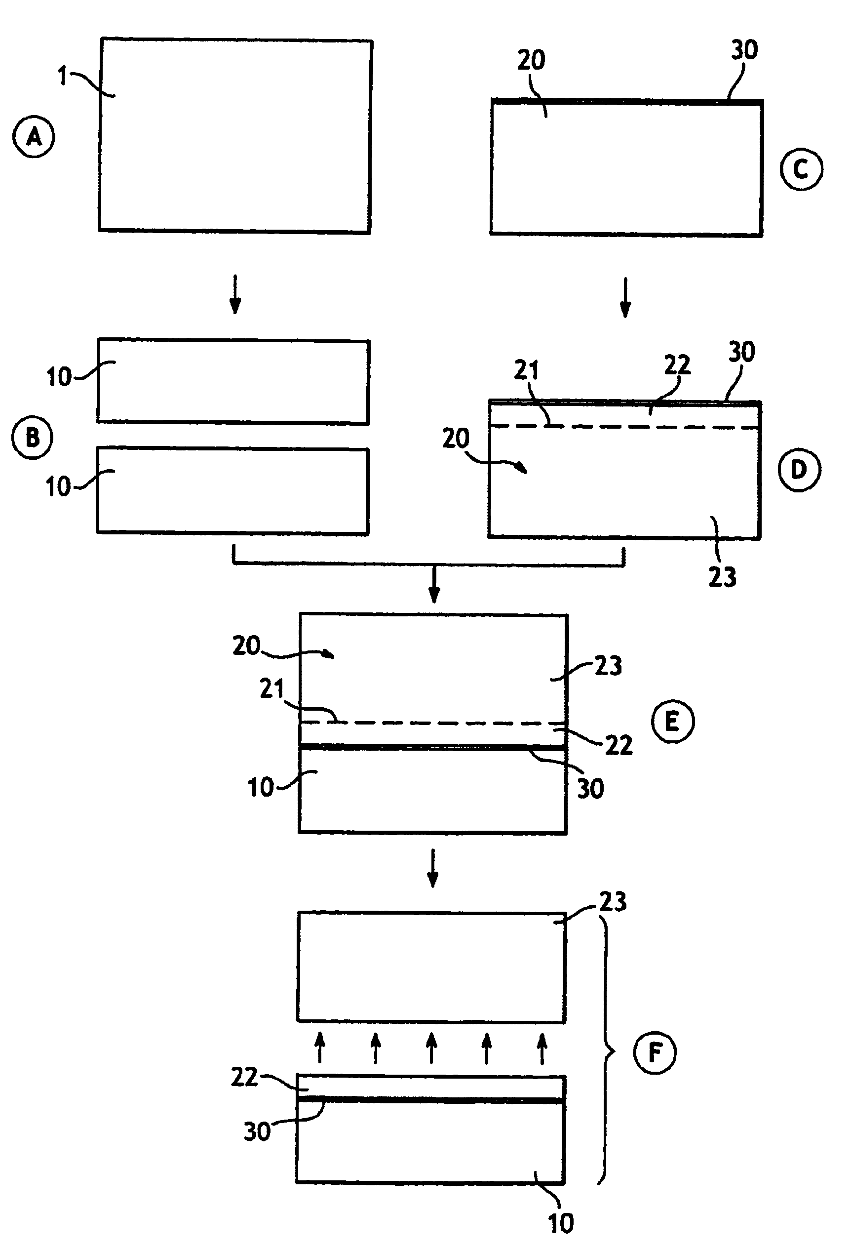
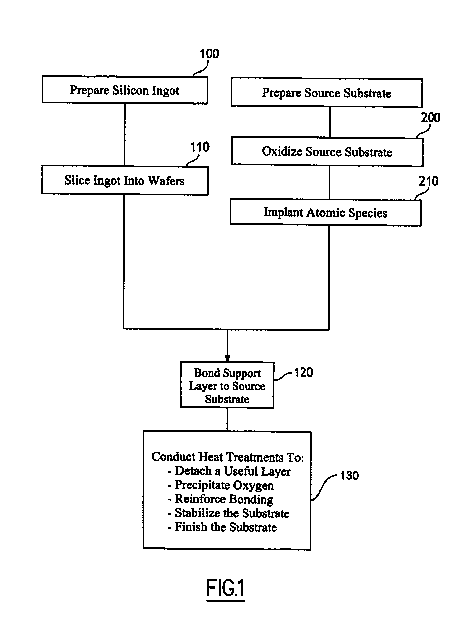
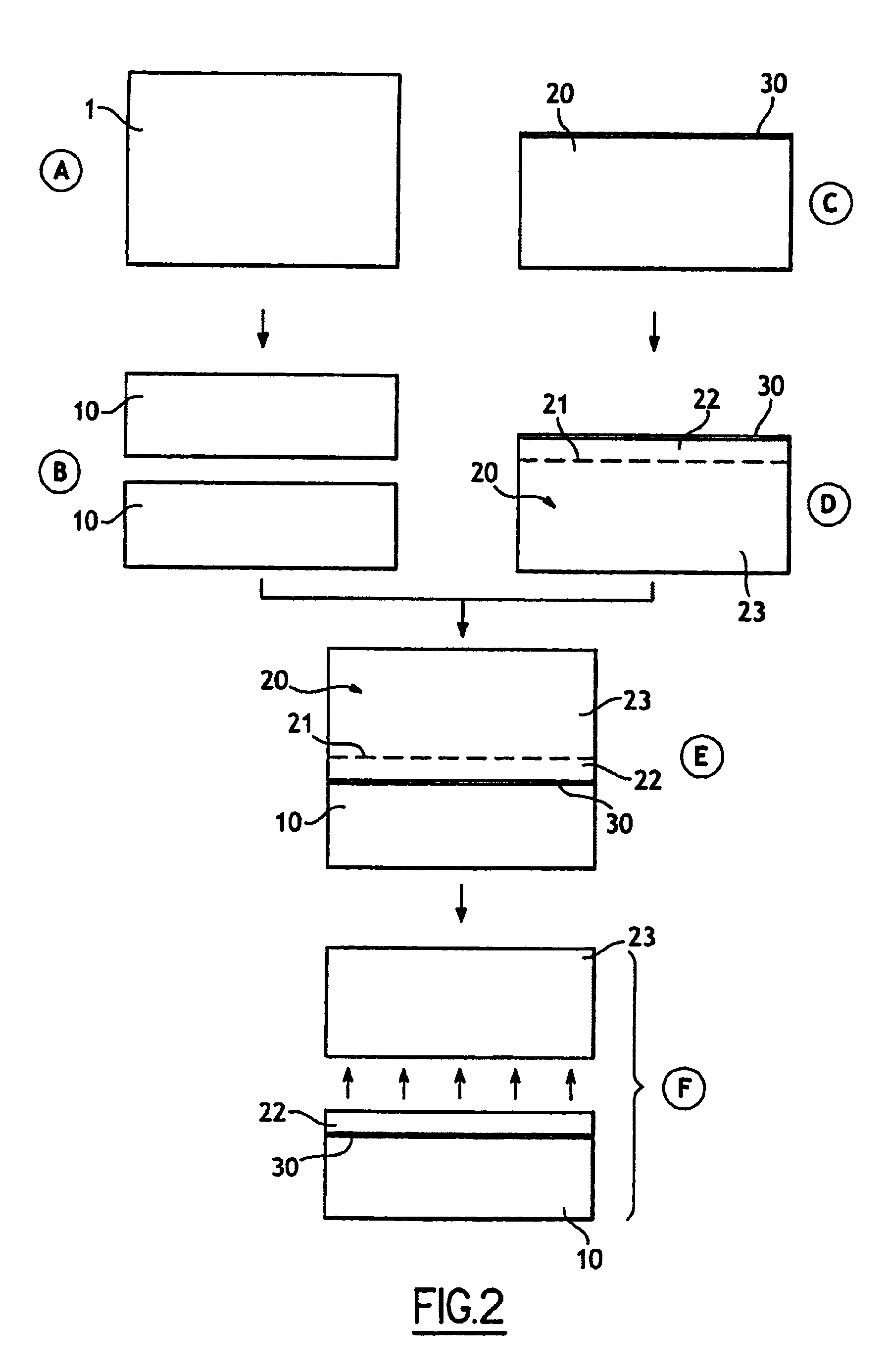
[0020]FIG. 1 is a diagram of the steps in a substrate fabrication method, and FIGS. 2A–2F are simplified block diagrams of the different states of the semiconductor material during implementation of the method. In FIG. 2A a Czochralski (CZ), Magnetic Field Applied Czochralski (MCZ), or like silicon ingot 1 is grown using a conventional technique (see also FIG. 1, step 100). The ingot pulling conditions are such that a certain concentration of interstitial oxygen exists in the material which is formed. In accordance with the present invention, the concentration of interstitial oxygen must be sufficient (of the order of 12 to 14 new ppma in a standard CZ substrate) to guarantee that a minimum concentration of oxygen precipitates is formed after carrying out the heat treatment.

[0021]The ingot 1 is sliced (step 110) by sawing it into wafers 10 (FIG. 2B) of a given thickness and then polished using techniques that are well known to the skilled person. FIG. 2B illustrates a first implemen...


PUM


Abstract

A method for limiting slip lines in a semiconductor substrate including a support layer and a useful semiconductor layer that is transferred to the support layer. The method includes precipitating at least a portion of interstitial oxygen in the support layer by a series of heat treatments conducted after bonding of the useful semiconductor layer to the support layer. The heat treatments occur at a temperature and a time sufficient to reduce the generation of slip lines therein.

Description

BACKGROUND ART[0001]The present invention generally relates to the production of composite substrates based on silicon, such as silicon on insulator (SOI) type substrates.[0002]It is known to fabricate a substrate by transferring a thin semiconductor layer onto a base substrate acting as a massive support that initially has a non-zero quantity of interstitial oxygen. For example, such a method is used to produce support substrates having high resistivity. To achieve this end, the interstitial oxygen present in the base substrate is precipitated to reduce the quantity of residual oxygen. i.e. the oxygen remaining after precipitation). Studies in this area have shown that a high resistivity substrate may be obtained by achieving a residual oxygen content Oi which is as low as possible. Such substrates may be used in the field of microwave applications. In particular, integrating high quality factor, passive components implies limiting high frequency losses by eddy currents, which can ...

Claims


Application Information

Patent Timeline
Patent Type & Authority Patents(United States)
IPC IPC(8): H01L21/425H01L21/762
CPCH01L21/76254
Inventor NEYRET, ERIC
Owner SOITEC SA
Why Eureka
Try Eureka