Compensation circuit for amplifiers having multiple stages

a technology of compensating circuit and amplifier, which is applied in the field of amplifiers, can solve the problems of becoming more difficult to supply voltage to the required transistor, and achieving additional bandwidth increases,

Active Publication Date: 2006-02-21
MARVELL ASIA PTE LTD
View PDF13 Cites 43 Cited by
  • Summary
  • Abstract
  • Description
  • Claims
  • Application Information

AI Technical Summary

Benefits of technology

[0021]In still other features, a load capacitance has one end that communicates with an output of the second amplifier stage. A first impedance has one end that communicates with the input of the first amplifier stage. A second impedance has one end that communicates with the input of the first amplifier stage and an opposite end that communicates with the output of the second amplifier stage. The first and second impedances are at least one of a resistance, a capacitance and a short circuit.
[0022]A broadband inverter comprises a first transistor having a control terminal and first and second terminals. A second transistor has a control terminal, a first terminal that communicates with the second terminal of the first transistor, and a second terminal. Third, fourth, and fifth transistors each have a control terminal and first and second terminals. The control terminal of the third transistor communicates with the control terminal of the second transistor. The first terminal of the third transistor communicates with the control terminal of the fourth transistor. The first terminal of the fourth transistor communicates with the control terminal of the fifth transistor. The first terminal of the first transistor communicates with the first terminal of the fifth transistor. A resistance has one end that communicates with the first terminal of the third transistor and an opposite end that communicates with the first terminal of the fourth transistor. A feedback capacitance has one end that communicates with the first terminal of the first transistor and an opposite end that communicates with the control terminals of the second and third transistors.
[0023]In other features, the first transistor is a PMOS transistor, the control terminal of the first transistor is a gate, the first terminal of the first transistor is a source and the second terminal of the first transistor is a drain.
[0024]In other features, the second, third, fourth and fifth transistors are NMOS transistors, the control terminals of the second, third, fourth and fifth transistors are gates, the first terminals of the second, third, fourth and fifth transistors are sources and the second terminals of the second, third, fourth and fifth transistors are drains.

Problems solved by technology

Because power supply voltage levels have been reduced to decrease the power dissipation of a host device, it has become more difficult to supply voltage to the required transistors when they are arranged in a single amplifier stage.
While the Miller compensation capacitor Cm increases the bandwidth of the two stage amplifier, additional increases in bandwidth are very difficult to achieve.

Method used


Image

  • Compensation circuit for amplifiers having multiple stages
  • Compensation circuit for amplifiers having multiple stages
  • Compensation circuit for amplifiers having multiple stages

Examples


Embodiment Construction

[0045]The following description of the preferred embodiment(s) is merely exemplary in nature and is in no way intended to limit the invention, its application, or uses. For purposes of clarity, the same reference numbers will be used in the drawings to identify similar elements.

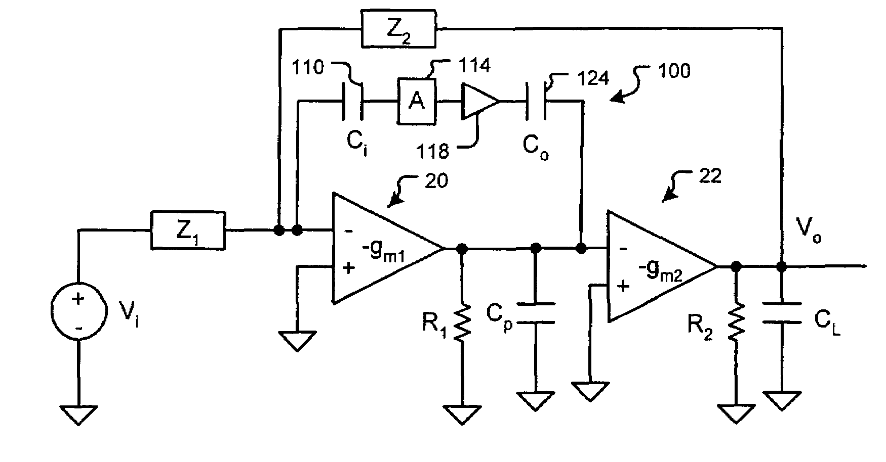
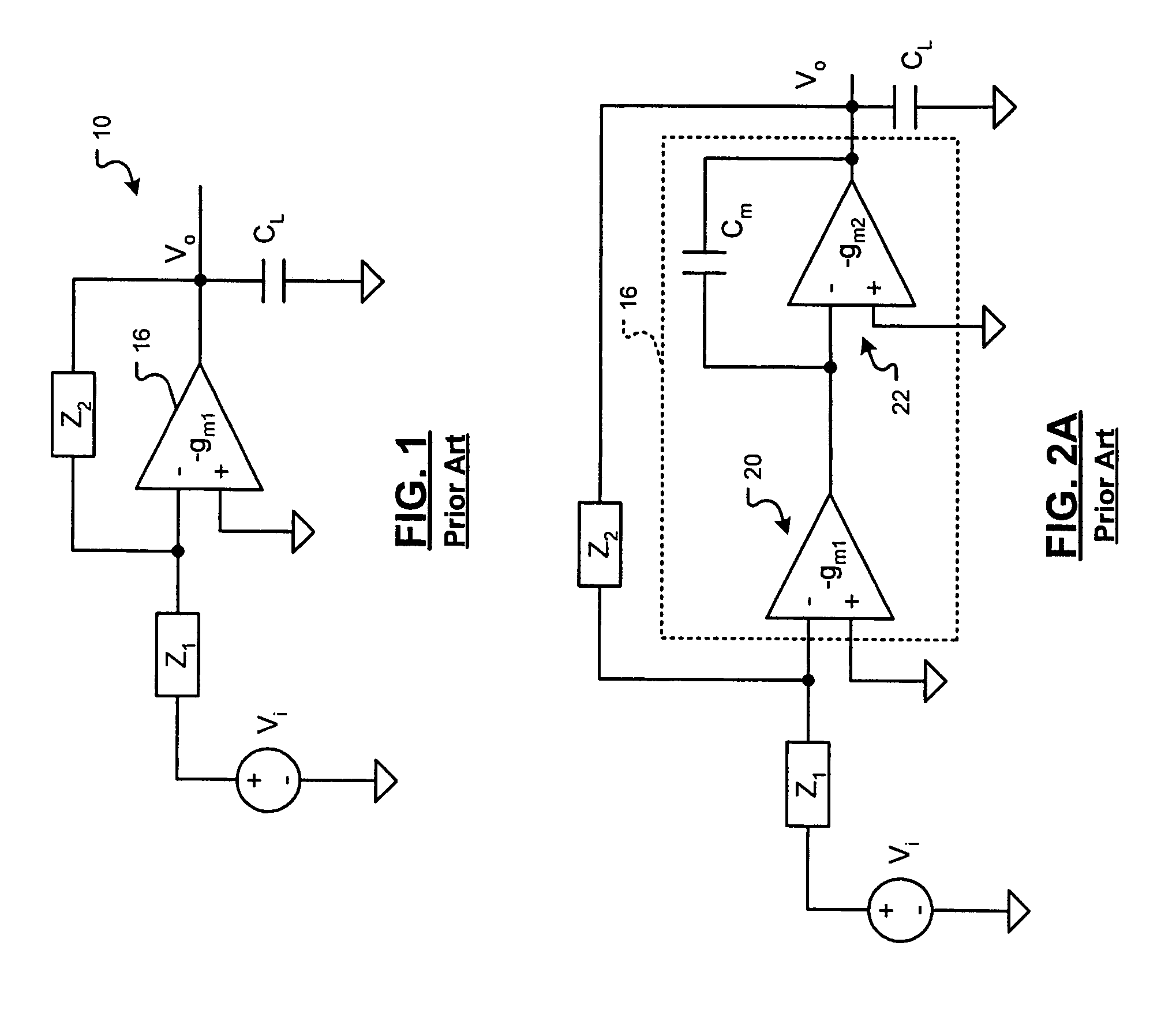
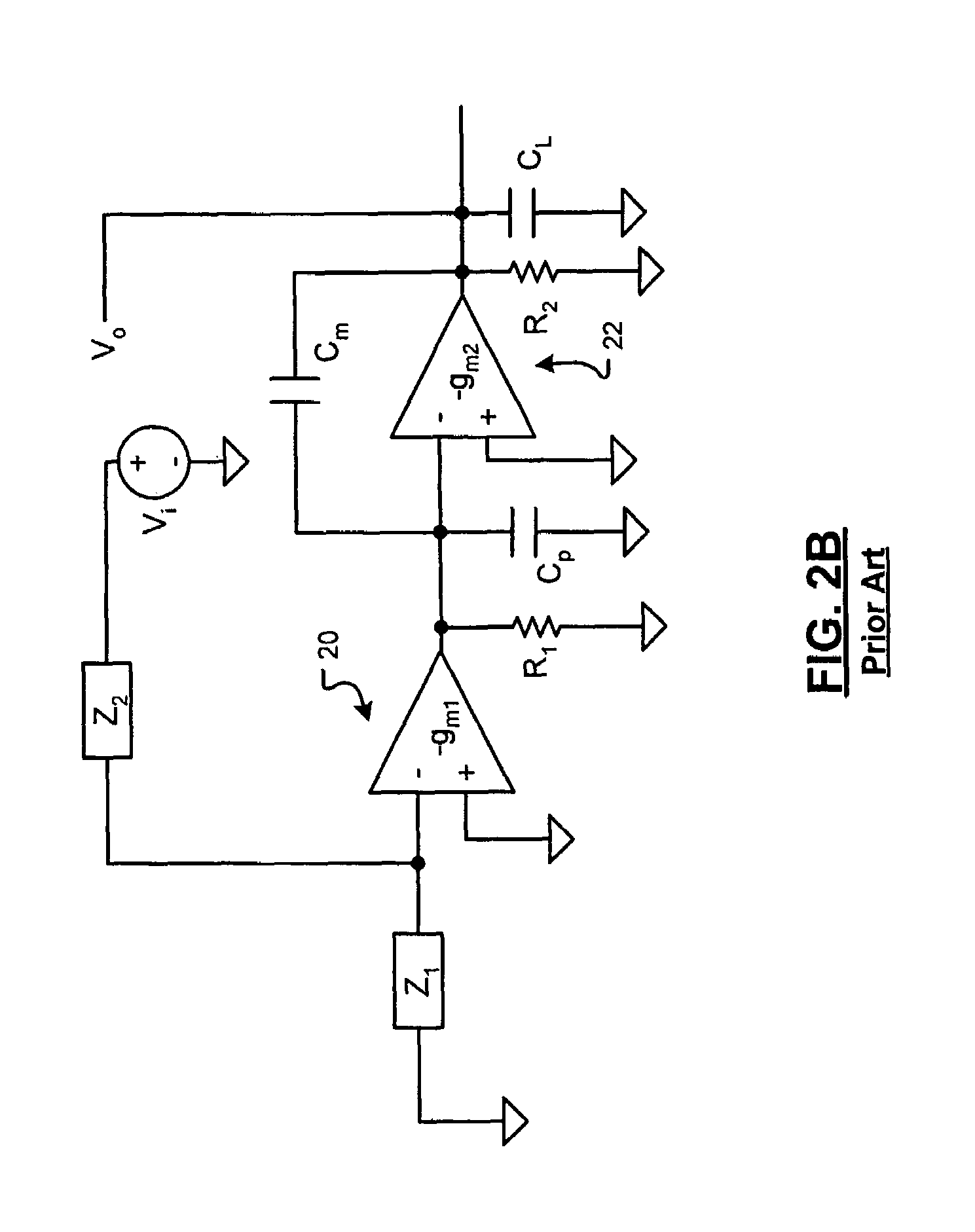
[0046]Referring now to FIG. 8, a compensation circuit according to the present invention is shown for an amplifier circuit that includes two or more stages. The amplifier 16 is shown to include the first amplifier stage 20 having a first transconductance gm1 and the second amplifier stage 22 having a second transconductance gm2. The internal resistances R1 and R2 and a parasitic capacitance Cp of the second amplifier stage 22 are shown. The load capacitance CL is connected to the output of the second amplifier stage 22.

[0047]The compensation circuit 100 includes an input capacitance Ci 110 having one end that is coupled to the inverting input of the first amplifier stage 20. An opposite end of the input capac...


PUM


Abstract

A compensation circuit is provided for an amplifier including at least first and second amplifier stage. The circuit includes a first capacitance including one end that communicates with an input of the first amplifier stage. An amplifier includes a first gain, an input that communicates with an opposite end of the first capacitance, and an output. A second capacitance includes a first end that communicates with the output of the amplifier and an opposite end that communicates with an input of the second amplifier stage. A first impedence includes one end that communicates with the input of the first amplifier stage and an opposite end that communicates with an output of the second amplifier stage.

Description

FIELD OF THE INVENTION[0001]The present invention relates to amplifiers, and more particularly to compensation circuits for amplifiers having two or more stages.BACKGROUND OF THE INVENTION[0002]Referring now to FIG. 1, an amplifier circuit 10 without compensation is shown. A voltage source Vi delivers voltage through an impedance Z1 to an inverting input of an amplifier 16. A non-inverting input of the amplifier 16 is coupled to a reference potential such as ground. The inverting input of the amplifier 16 is coupled through a feedback impedance Z2 to an output of the amplifier 16. A load capacitance CL is coupled to the output of the amplifier 16. An output voltage VO is taken at the output of the amplifier 16. The impedances Z1 and Z2 can be resistive, capacitive and / or short circuits.[0003]Because power supply voltage levels have been reduced to decrease the power dissipation of a host device, it has become more difficult to supply voltage to the required transistors when they are...

Claims


Application Information

Patent Timeline
Patent Type & Authority Patents(United States)
IPC IPC(8): H03F1/24
CPCH03F3/68H03F1/08
Inventor ARAM, FARBOD
Owner MARVELL ASIA PTE LTD
Why Eureka
Try Eureka