Image forming apparatus

a technology of image forming apparatus and forming head, which is applied in the field of writing head, can solve the problems of deterioration of print quality, affecting the quality of final image, so as to achieve uniform electrostatic latent image, high quality, and stable image.

Inactive Publication Date: 2006-02-21
SEIKO EPSON CORP
View PDF8 Cites 2 Cited by
  • Summary
  • Abstract
  • Description
  • Claims
  • Application Information

AI Technical Summary

Benefits of technology

[0015]It is therefore an object of the invention to provide a writing head device capable of eliminating bending and creasing thereof due to the stress concentration, and enabling writing electrodes in individual arrays to stably and evenly contact with a latent the image carrier.
[0026]According to the above configurations, the stiffness of the portion between the two electrode arrays can be increased to stabilize the contact condition of the writing electrodes with respect to the image carrier. As a result the fluctuation of the distance between writing electrodes in the individual arrays can be avoided so that the occurrence of horizontal streaks in the final image can be eliminated.
[0035]According to the above configurations, the contact pressure between electrode arrays and the image carrier can be effectively made equal. Therefore, the contact resistance of each electrode array with respect to the image carrier is made equal, enabling the consistent formation of high quality electrostatic latent images on the image carrier.
[0036]Further, since the same voltage can be applied to every electrode array, the voltage control can be facilitated and the use of a high-voltage IC can be avoided.
[0053]According to the above configurations, the difference between the contact forces of the writing electrodes with respect to the image carrier is canceled. Since the contact resistances of the writing electrodes with respect to the image carrier are made substantially identical with each other, an uniform electrostatic latent image can be formed. Performing the normal or reversal development with this uniform latent image, a final image with high quality can be stably obtained.

Problems solved by technology

Such an image forming apparatus is likely to be bulky and has a complicated configuration since the exposing device for writing electrostatic latent images must be provided with a light generator.
As a result, electrostatic latent images cannot be correctly formed on the latent the image carrier, causing the deterioration of print quality.
Moreover, another problem takes place that the creasing and bending of the writing head act to fluctuate the spacing between the two arrays of writing electrode, and thus giving horizontal streaks in the final image due to pitch fluctuation in the electrostatic latent image.
In the second related art, it cannot sufficiently prevent the bending and creasing of the writing head because the writing head is pressed with an extremely weak load.
In a case where the writing operation is performed by applying the same voltage to the two electrode arrays having different contact resistances, the latent image is deteriorated.

Method used


Image

  • Image forming apparatus
  • Image forming apparatus
  • Image forming apparatus

Examples


first embodiment

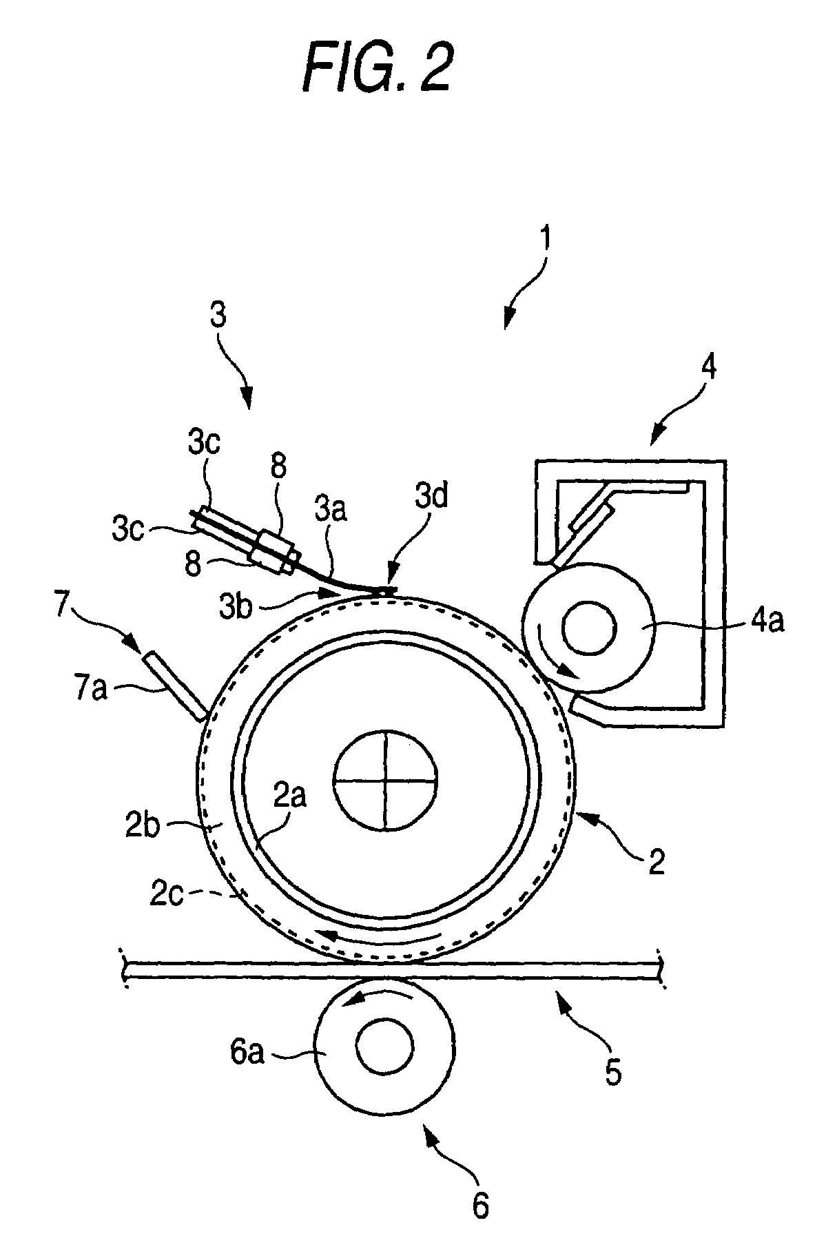
[0082]FIG. 2 shows an image forming apparatus according to the invention. The image forming apparatus 1 comprises: a rotatable the image carrier 2 on which an electrostatic latent image and a developer image are formed; a writing device 3 which is brought into contact with the image carrier 2 to write the latent image thereon; a developing device 4 which develops the electrostatic latent image on the image carrier 2 with developer (e.g., toner) held oh and carried by a developing roller 4a; a transferring device 6 which transfers the developer image from the image carrier 2 onto a recording medium 5 such as paper; and a cleaner 7 having a cleaning blade 7a which cleans the surface of the image carrier 2 by removing the toner remaining on the image carrier 2 after the transferring operation.

[0083]In this case, development of an electrostatic latent image is of the normal type, and the toner used for the development may be either positively or negatively charged.

[0084]The explanation ...

second embodiment

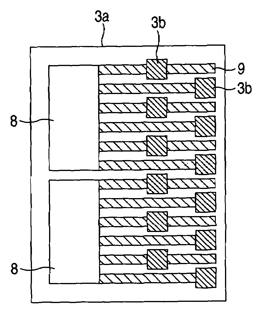
[0099]FIGS. 4B and 5B show the invention in which driver ICs 8 are disposed at both sides of the two electrode arrays in the advancing direction of the image carrier 2.

[0100]In this embodiment, since all the wiring patterns 9 are extended through the writing electrodes 3b from one side to another. The number of wiring patterns 9 arranged between the two electrode arrays is made twice of the number of wiring patterns 9 extended from the drivers 8 of one side. Therefore, the stiffness of the portion between the two electrodes arrays are made greater than other portions.

[0101]In order to make the stiffness even in the entire region of the wiring device, the extended portions of the wiring patterns 9 from the drivers 8 of one side may be omitted so that the number of wiring patterns 9 arranged between the two electrode arrays is made identical with the number of wiring patterns 9 extended from the drivers 8.

third embodiment

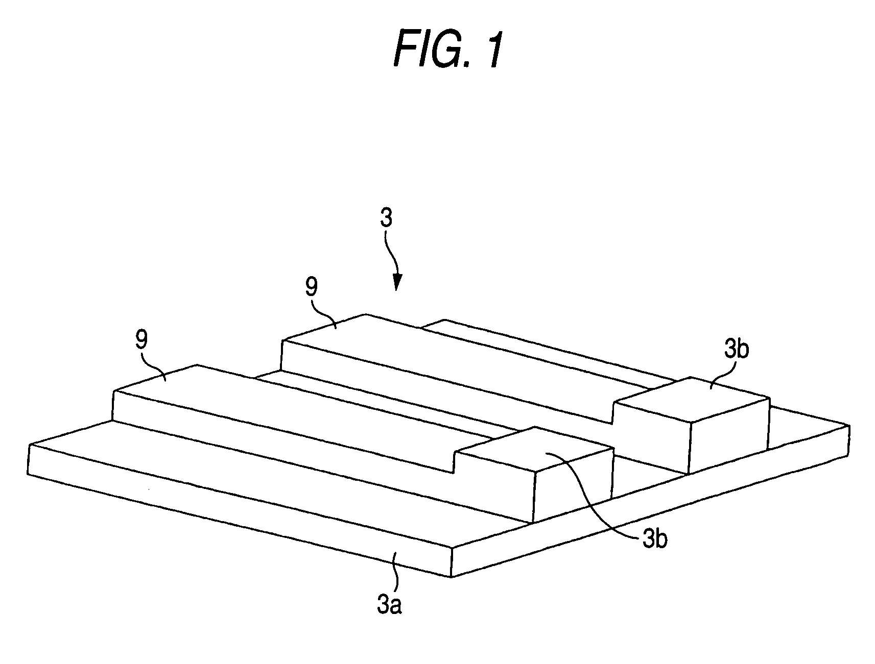
[0102]FIG. 6A shows the invention, in which the writing electrodes 3b are arranged so as to form three electrode arrays.


PUM


Abstract

A head device is for writing an electrostatic latent image on an image carrier of an image forming apparatus which is movable in a first direction. In the head device, a plurality of writing electrodes are arrayed on a substrate in a second direction perpendicular to the first direction to form a plurality of electrode arrays which are arranged in the first direction. The writing electrodes are brought into contact with the image carrier with a flexibility of the substrate. A head driver is disposed on the substrate. A plurality of wirings are extending in the first direction to connect the head driver and the respective writing electrodes to supply writing voltages from the head driver to the writing electrodes. At least one of the wirings extended through one of the writing electrodes in one of the electrode arrays is placed between adjacent ones of the writing electrodes in another one of the electrode arrays.

Description

BACKGROUND OF THE INVENTION[0001]The present invention relates to a writing head in which plural arrays of writing electrode are formed on a flexible substrate for forming an electrostatic latent image on a latent the image carrier by applying a writing voltage to the electrode from a head driver. The present invention also relates to an image forming apparatus provided with the writing head.[0002]In an image forming apparatus such as an electrostatic copying machine, a printer, the surface of a photosensitive member is uniformly charged by a charging device, and by exposing light from an exposing device such as a laser or an LED, an electrostatic latent image is formed in the surface of the photosensitive member. Thereafter, through the development of the electrostatic latent image in the surface of the photosensitive member, a developer image is formed on the surface of the photosensitive member. This developer image is transferred to a recording medium such as paper by a transfer...

Claims


Application Information

Patent Timeline
Patent Type & Authority Patents(United States)
IPC IPC(8): B41J2/395
CPCB41J2/395
Inventor KAMOSHIDA, SHINICHIKATSUKI, KIYOTERU
Owner SEIKO EPSON CORP
Why Eureka
Try Eureka