Printed wiring board

A technology of printed circuit boards and wiring substrates, which is applied in the direction of printed circuits, printed circuits, printed circuit manufacturing, etc., can solve the problems of insulation reliability reduction, connection reliability, insulation reliability reduction, connection reliability reduction, etc., to prevent Reduced insulation resistance, improved connection reliability, and improved insulation reliability

Active Publication Date: 2008-04-30
IBIDEN CO LTD
View PDF4 Cites 7 Cited by
  • Summary
  • Abstract
  • Description
  • Claims
  • Application Information

AI Technical Summary

Problems solved by technology

If such gaps appear, flux residues or cleaning solution residues tend to remain in the gaps, so in printed wiring boards with a conductor land pitch of 200 μm or less, insulation reliability is likely to decrease
Moreover, such residues will lead to a decrease in the adhesion force, so that the peeling of the solder resist and the underfill material will easily occur, resulting in a decrease in connection reliability.
In addition, since it becomes difficult to fill the underfill material, if a large IC chip is to be mounted, holes are likely to be mixed in the underfill material, reducing connection reliability and insulation reliability.

Method used


Image

  • Printed wiring board
  • Printed wiring board
  • Printed wiring board

Examples


Embodiment 1

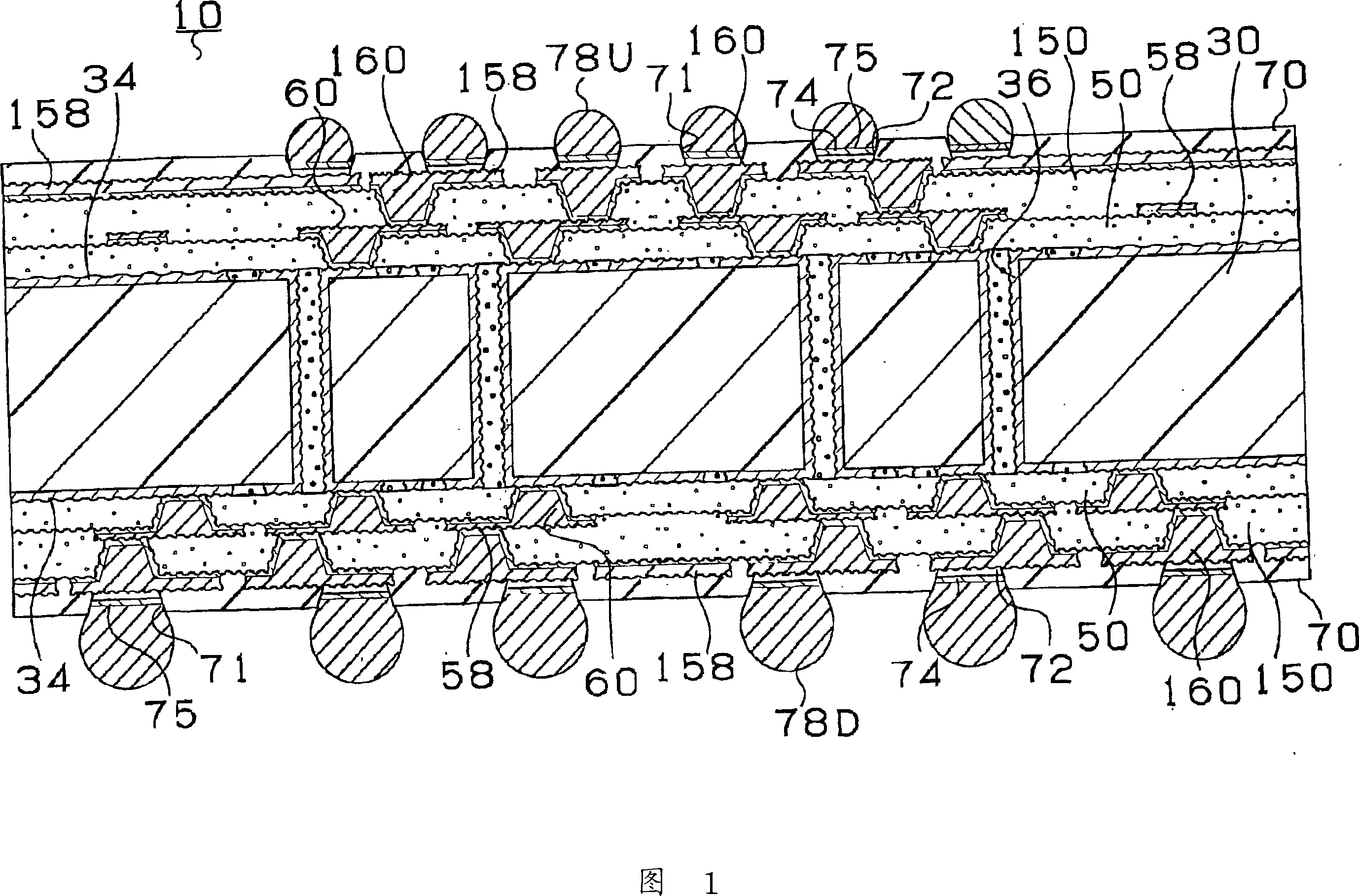
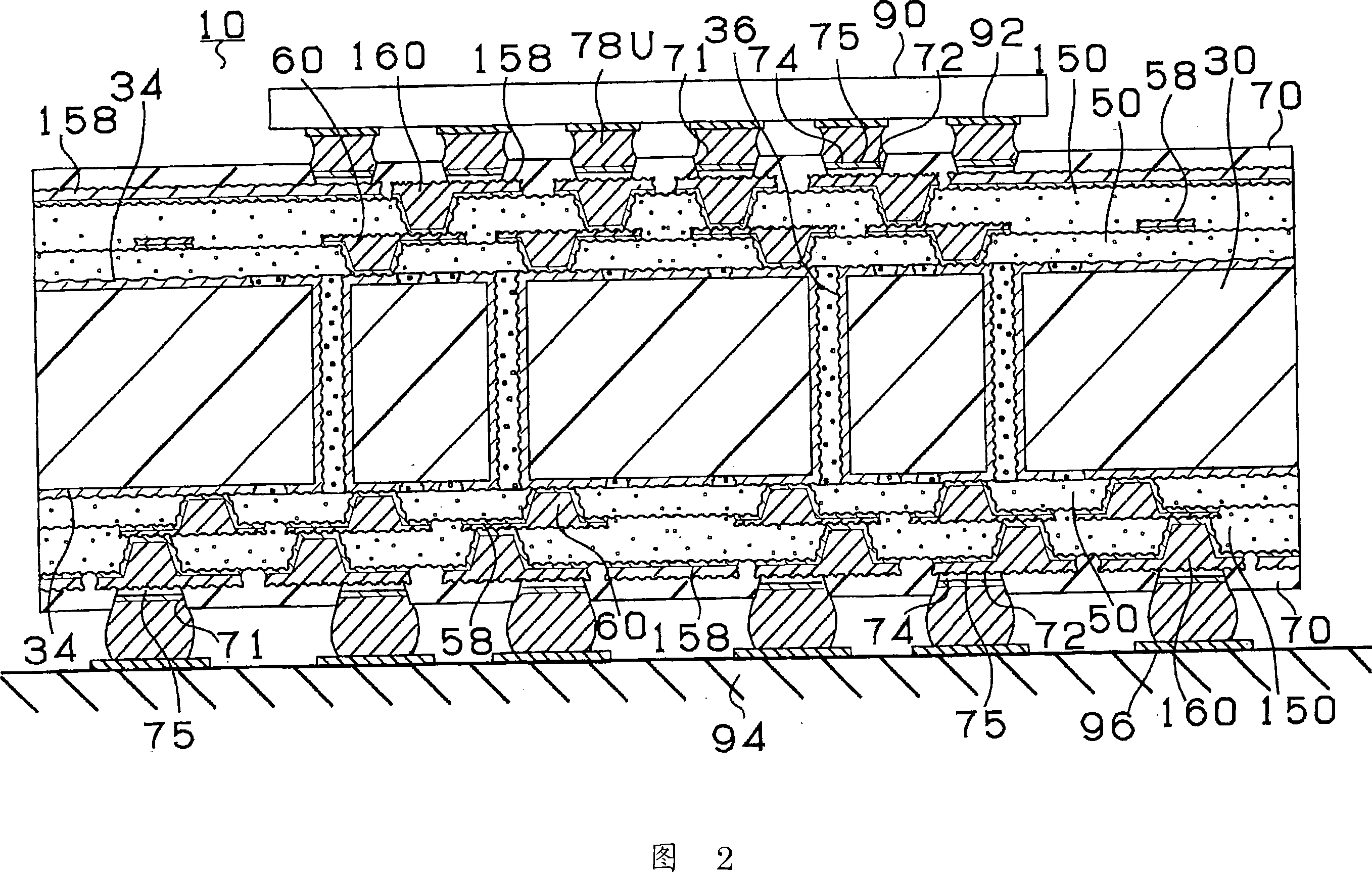
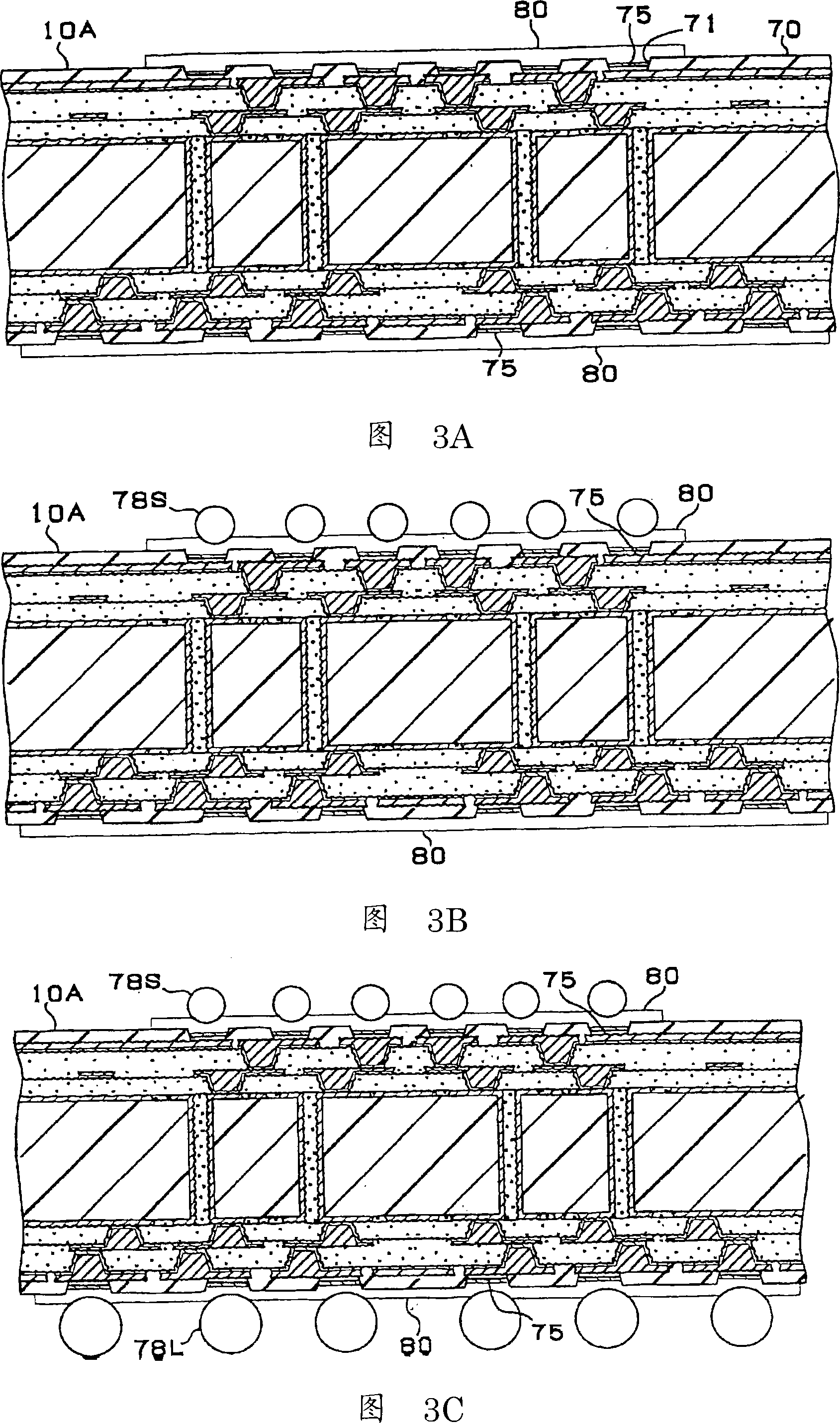
[0094] (1) Production of printed circuit boards

[0095] A double-sided copper-clad laminate (for example, "MCL-E-67" manufactured by Hitachi Chemical Industries, Ltd.) is used as a starting material, and through-hole conductors and conductor circuits are formed on this substrate by a known method. Thereafter, interlayer insulating layers and conductor circuit layers are alternately laminated by a known method (such as "Build-up Multilayer Printed Wiring Board" (written by Kiyoshi Takagi) issued by Nikkan Kogyo Shimbun on June 20, 2000), and at the end In the conductor circuit layer of the outer layer, within 150mm 2 In the connection pad region, a group of connection pads for IC chip mounting consisting of 50×40 connection pads (arranged in a grid) with a thickness of 20 μm, a diameter (connection pad diameter): 120 μm, and a pitch of 150 μm is formed.

[0096] Such connection pads are formed, for example, by the same method as described in JP-A-2000-357762.

[0097] In add...

Embodiment 2

[0130] A printed wiring board was produced in the same manner as in Example 1 except that solder balls having a diameter of 100 μm were mounted. As a result, the solder bump diameter was 100 μm.

Embodiment 3

[0132] A printed wiring board was produced in the same manner as in Example 1 except that solder balls with a diameter of 120 μm were mounted. As a result, the solder bump diameter was 120 μm.


PUM


Abstract

A printed wiring board comprises a wiring substrate provided with at least one conductor circuit, a solder resist layer provided on the surface of the wiring substrate, at least one conductor pad formed from a part of the conductor circuit exposed from an opening provided in the solder resist layer, and at least one solder bump for mounting electronic parts on the conductor pad. In the printed wiring board, since the at least one conductor pad is aligned at a pitch of 200 µm or less, and a ratio (W/D) of a diameter W of the solder bump to an opening diameter D of the opening formed in the solder resist layer is within a range of 1.05 to 1.7, connection reliability and insulation reliability can be easily improved.

Description

technical field [0001] The present invention relates to a printed wiring board on which electronic components such as capacitors and ICs are mounted on the surface. Specifically, it relates to a printed wiring board suitable for narrowing the pitch of solder bumps for mounting electronic components. Background technique [0002] When mounting semiconductor elements such as IC chips on a printed wiring board, first, solder bumps are formed on the semiconductor element mounting pads (hereinafter simply referred to as "conductor pads") formed on the printed wiring board. Cover a portion of the conductor pad with a solder mask, leaving only the central portion of the conductor pad exposed. In order to form solder bumps on such conductor pads, the printed wiring board is first set on a solder paste printer, and then a mask for solder printing such as a metal mask or a plastic mask is laminated on the printed wiring board (with the The conductor pads on the board are provided wit...

Claims


Application Information

Patent Timeline
Patent Type & Authority Applications(China)
IPC IPC(8): H05K3/34H01L21/60H05K3/28
CPCB23K3/0623B23K2201/42H01L2924/15174H01L2224/11334H01L24/81H01L2924/15311H01L2224/81815H01L2224/16H01L2223/54473H05K2201/0191H01L23/544H01L21/4853H01L2924/01079H01L2924/01019H05K3/3452H01L2924/0102H01L2924/01078H05K2203/041H05K2203/0557H01L2224/8121H05K3/3478H05K2201/099H01L2224/81192H01L23/49811H01L2224/81801B23K2101/42H01L2224/05568H01L2224/05573H01L2224/16225H01L2924/00014H01L2924/12042H01L2924/14H01L2924/00H01L2224/05599H05K3/28H05K3/34
Inventor 川村洋一郎泽茂树丹野克彦田中宏德藤井直明
Owner IBIDEN CO LTD
Why Eureka
Try Eureka