Light receiving amplification element

a technology of light receiving and amplifier, which is applied in the field of light receiving amplifier, can solve the problems of increasing the number of parts, increasing the cost of progress related to the development of the project, and increasing the complexity of the optical design, so as to reduce the cost of chips caused by the increase of the scale of the circuit, reduce the cost of chips, and prevent the effect of saturation

Inactive Publication Date: 2006-02-21
SHARP KK
View PDF4 Cites 27 Cited by
  • Summary
  • Abstract
  • Description
  • Claims
  • Application Information

AI Technical Summary

Benefits of technology

[0057]In addition, it is preferable that the first feedback constant (gain resistance) is set for reproduction and the second feedback constant is set for rewriting respectively and a clamp circuit comprising diode and resistance is connected in parallel to a second feedback circuit. Thereby, at the time of inputting large quantity of light for writing operation, amplifier gain is lowered and saturation of the light receiving portion can be prevented and therefore light receiving amplifier characteristics adaptable to reproduction and rewriting can be obtained in both cases of two different wavelengths.
[0058]In addition, it is preferable that the two trans-impedance type amplifiers (pre-amplifiers) connected to the above-mentioned two light receiving portions respectively comprise two differential elements (first and second differential elements), a single current mirror circuit in which collectors are connected to each other as output of the differential elements and which acts as an active load, an emitter follower output circuit, and two feedback circuits. Thereby the two pre-amplifiers have one output terminal and an output signal is outputted from the output terminal with voltage further amplified by one post-amplifier and therefore only one post-amplifier with only one external output terminal is required for the two light receiving portions and increase of cost of chips caused by increase of a scale of a circuit can be restrained and furthermore there is no increase of the external output terminals (i.e. pins). Consequently, increase of cost of the light receiving amplifier element including a package can be restrained.
[0059]In addition, it is preferable that bias current of each of the differential elements configuring the trans-impedance type amplifiers is switched between ON and OFF states as switching means for the two trans-impedance type amplifiers. Thereby a trans-impedance type amplifier corresponding to each wavelength performs active selection, and therefore switching function can be realized by a small number of elements and increase of cost caused by increase of a chip area can be restrained.
[0060]In addition, it is preferable that the two light receiving portions corresponding to the two wavelengths respectively are formed on the same substrate on which the amplifying circuit is formed. Thereby accuracy of positions of the two light receiving portions corresponding to each of wavelengths can be enhanced by using technique of semiconductor photograph.
[0061]Furthermore, the distance between the two receiving light portions is adapted to the distance between emitting points for each wavelength of the semiconductor two-wavelength laser element to be used and thereby satisfactory light receiving characteristics can be obtained.
[0062]The light receiving amplification element is configured so that one output is obtained by switching two light receiving portions adapted to the distance between the light emitting points of the semiconductor two-wavelength laser which outputs the laser light having two different wavelengths from one chip and the trans-impedance type amplifiers which are connected to the two light receiving portions respectively, thereby the invention can provide the light receiving amplification element adaptable to the optical pickup apparatus using the semiconductor two-wavelength laser.

Problems solved by technology

Consequently, since optical design including the semiconductor laser element is complicated and there is necessity of a mechanism available for switching the optical system between the two wavelengths, the optical design becomes more complicated and the number of parts is increased and there is progress related cost is also increased.

Method used


Image

  • Light receiving amplification element
  • Light receiving amplification element
  • Light receiving amplification element

Examples


embodiment 1

(Embodiment 1)

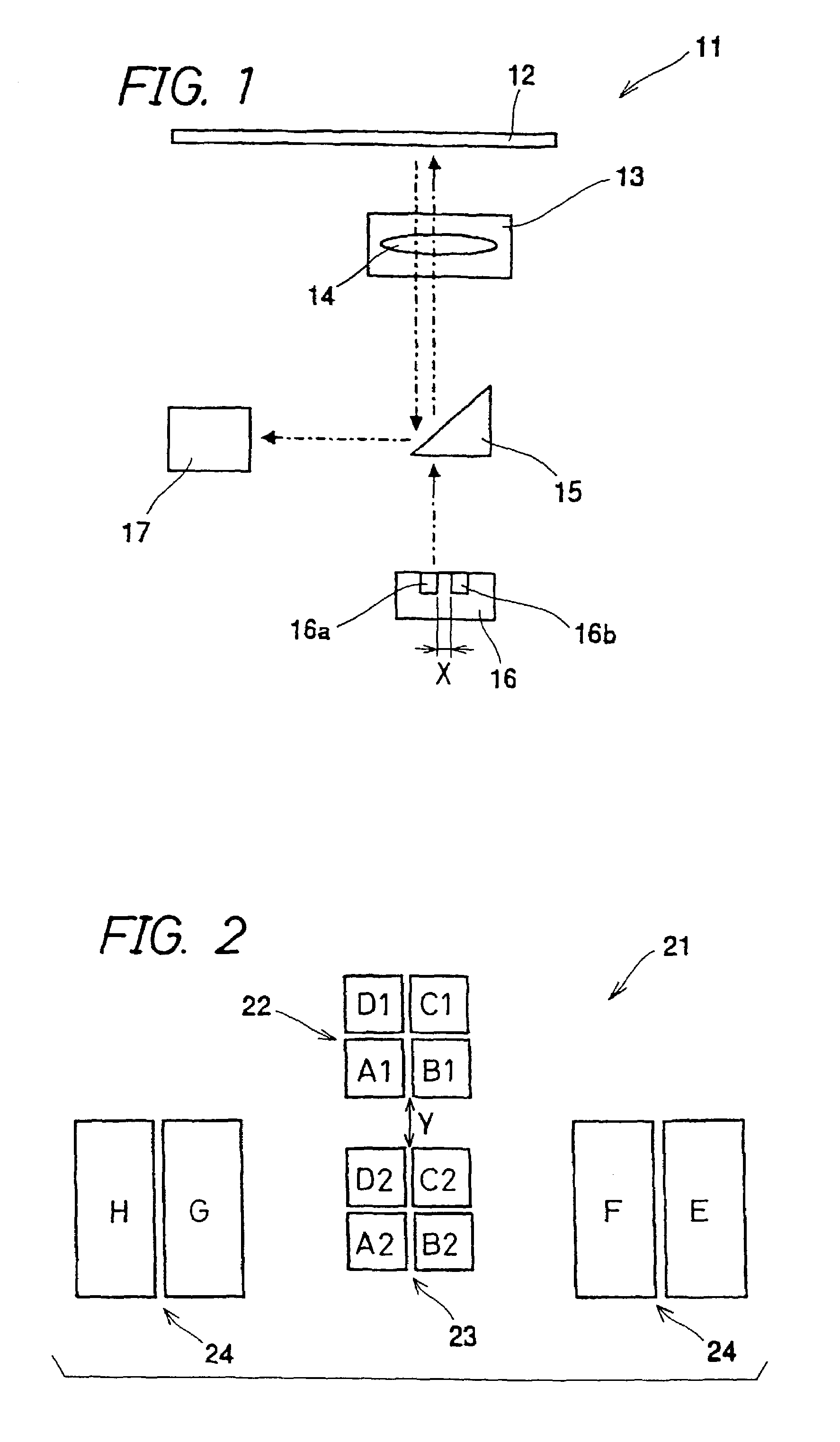
[0076]FIG. 1 is a side view of the optical pickup apparatus in the embodiment 1 of the invention.

[0077]Referring to FIG. 1, an optical pickup apparatus 11 is provided with a semiconductor two-wavelength laser element (hereinafter referred to as a two-wavelength laser) 16 which acts as a light source. The two-wavelength laser 16 forms two laser emitting points for different wavelengths on the same substrate. Reference numeral 16a denotes a first emitting point for DVD (650 nm wavelength) and reference numeral 16b denotes a second emitting point for CD (780 nm wavelength). An optical lens 13 comprising a prism 15 and a condensing lens 14 is arranged on a light path from the two-wavelength laser 16 to an optical disk 12. Furthermore, the optical pickup apparatus 11 is provided with a light receiving amplification element 17 having a light receiving portion for receiving laser light which is reflected by the optical disk 12 and is reflected by the prism 15 via the optical ...

embodiment 2

(Embodiment 2)

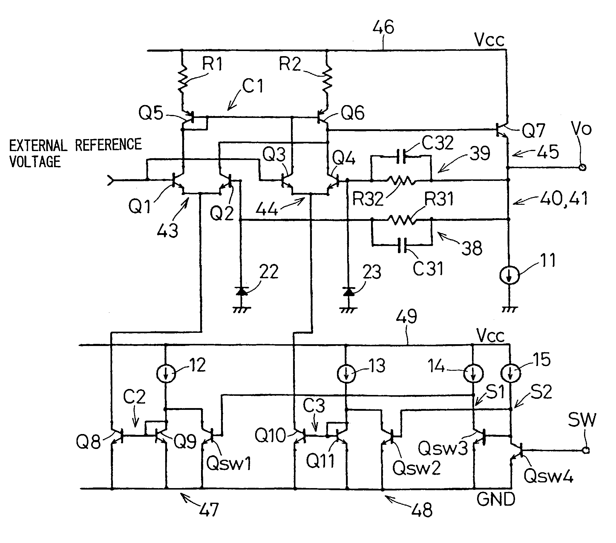
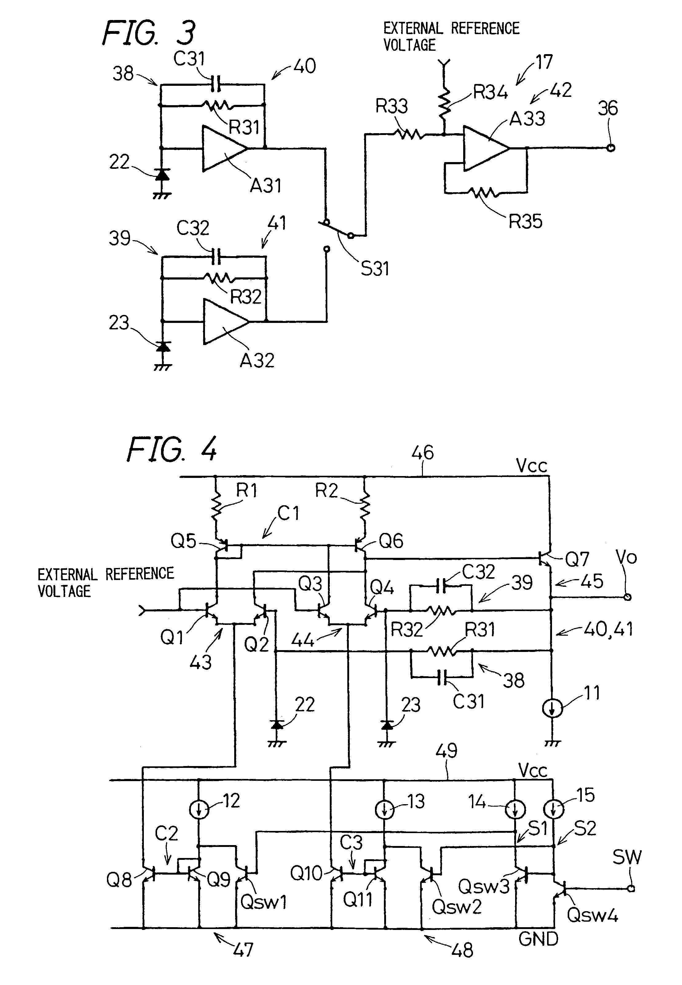
[0109]FIG. 5 is another equivalent circuit block diagram of the light receiving amplification element for outputting light signals sent from the two main light receiving portions corresponding to the two wavelengths in FIG. 2 as electric signals.

[0110]Here, the different points from FIG. 3 are as follows:

[0111]Output points of signals of the two light receiving portions 22 and 23 are connected to each other and output of signals of the two light receiving portions 22 and 23 are inputted to each of the two trans-impedance type amplifiers 40 and 41.

[0112]In addition, the values of the feedback resistances R31 and R32 are different in the two trans-impedance type amplifiers 40 and 41, and the value of the resistance R31 is set so as to be optimum sensitivity (i.e. gain) for a reproduction only optical disk having high reflectance, and the value of the resistance R32 is set so as to be optimum sensitivity (i.e. gain) for a rewritable optical disk having low reflectance. In...

embodiment 3

(Embodiment 3)

[0115]FIG. 6 is still another equivalent circuit block diagram of the light receiving amplification element for outputting light signals sent from the two main light receiving portions corresponding to the two wavelengths in FIG. 2 as electric signals.

[0116]Here, the different points from FIG. 5 are as follows:

[0117]In the feedback circuit 39 of the second trans-impedance type amplifiers 41a, a clamp circuit 50 comprising a resistance R36 and diodes D1 through D3 is connected in parallel with the second feedback resistance R32 and the second capacity C32, and the second feedback resistance R32 is set as sufficiently smaller value than the first resistance R31 so that the second feedback resistance R32 is adaptable to large quantity of light at the time of writing operation (R31>>R32).

[0118]The first trans-impedance type amplifiers 40 comprising the first amplifier A31, the first feedback resistance R31 and the first capacity C31 is set to be used for reproduction and t...


PUM

PropertyMeasurementUnit
wavelengthaaaaaaaaaa
wavelengthsaaaaaaaaaa

Abstract

The object of the invention is to provide a light receiving amplification element applicable to an optical pickup apparatus comprising a semiconductor two-wavelength laser element and one condensing lens. The light receiving amplification element is provided with a plurality of light receiving portions corresponding to different wavelengths, a plurality of trans-impedance type amplifiers connected to the light receiving portions according to the different wavelengths and adaptable to the different wavelengths and switching portion for switching output from the trans-impedance type amplifier according to each of the wavelengths.

Description

BACKGROUND OF THE INVENTION[0001]1. Field of the Invention[0002]The present invention relates to a light receiving amplification element to be used for an optical pickup apparatus using a semiconductor two-wavelength laser element which outputs light with two different wavelengths from one chip.[0003]2. Description of the Related Art[0004]Optical disks such as CD, DVD and the like are widely utilized as media on which a voice, an image, document data or the like is recorded and development is performed for various types of optical disk apparatuses which performs reproducing or recording the optical disk. An optical pickup apparatus is a main component for performing an input / output of a signal to / from the optical disk in a head portion of the optical disk apparatus.[0005]Since a DVD reproduction apparatus, which prevails rapidly in recent years, requires capability of reproducing an existing CD, the optical pickup apparatus requires two semiconductor laser elements having 650 nm wav...

Claims


Application Information

Patent Timeline
Patent Type & Authority Patents(United States)
IPC IPC(8): G11B7/00G11B7/005G11B7/125G11B7/1275G11B7/13G11B7/131
CPCG11B7/005G11B7/131G11B7/1275G11B2007/0006
Inventor OKUDA, TAKANORIOHNISHI, MASAYA
Owner SHARP KK
Why Eureka
Try Eureka