Group III nitride based semiconductor luminescent element

a technology of nitride and light-emitting elements, which is applied in the direction of semiconductor devices, semiconductor/solid-state device details, electrical apparatus, etc., can solve the problems of insufficient element function and solderability of electrodes, and achieve improved bonding strength between light-emitting elements and supports, improved adhesion, and stabilization of element functions

Inactive Publication Date: 2006-02-28
TOYODA GOSEI CO LTD
View PDF25 Cites 35 Cited by
  • Summary
  • Abstract
  • Description
  • Claims
  • Application Information

AI Technical Summary

Benefits of technology

[0007]In the aforementioned configuration, a film containing a material (Au) of an adhesive member (Au bump) used for mounting the light-emitting element on a support is formed on each of a surface of the p-side electrode and a surface of the n-side electrode to improve adhesion between each of the two electrode surfaces and the adhesive member. As a result, when the light-emitting element is mounted on the support, bonding strength between the light-emitting element and the support is improved. Accordingly, stabilization of the element function is attained and preservative characteristic or durability is improved.
[0008]Furthermore, because a film containing Au is formed on each of the two electrode surfaces, corrosion resistance of each of the two electrode surfaces is improved. It can be said from this point of view that a Group III nitride compound semiconductor light-emitting element high in preservative stability or durability is provided.
[0009]As described above, in accordance with the configuration of the invention, a light-emitting element excellent in preservative characteristic or durability and having a more stable element function is provided.
[0010]Incidentally, in the aforementioned configuration, because films the same in configuration are formed on the two electrode surfaces, the color tones of the two electrode surfaces can be matched with each other. Accordingly, there is also provided an effect of attaining improvement in appearance recognition of a surface of the light-emitting element on which the two electrodes are formed, improvement in mount accuracy at the time of mounting the support on the light-emitting element having the surface used as a mount surface, improvement in efficiency in the mounting process, etc.

Problems solved by technology

There is also fear that a sufficient element function cannot be exhibited because failure occurs in bonding between the n-side electrode and the support.
Furthermore, it is undesirable from the point of view of corrosion resistance that Al etc. which is the material of the electrode is exposed at the surface of the n-side electrode.
When the electrodes one of which is made of Al while the other is made of Au have to be soldered, there is a further problem in solderability of the electrodes.

Method used


Image

  • Group III nitride based semiconductor luminescent element
  • Group III nitride based semiconductor luminescent element
  • Group III nitride based semiconductor luminescent element

Examples


Embodiment Construction

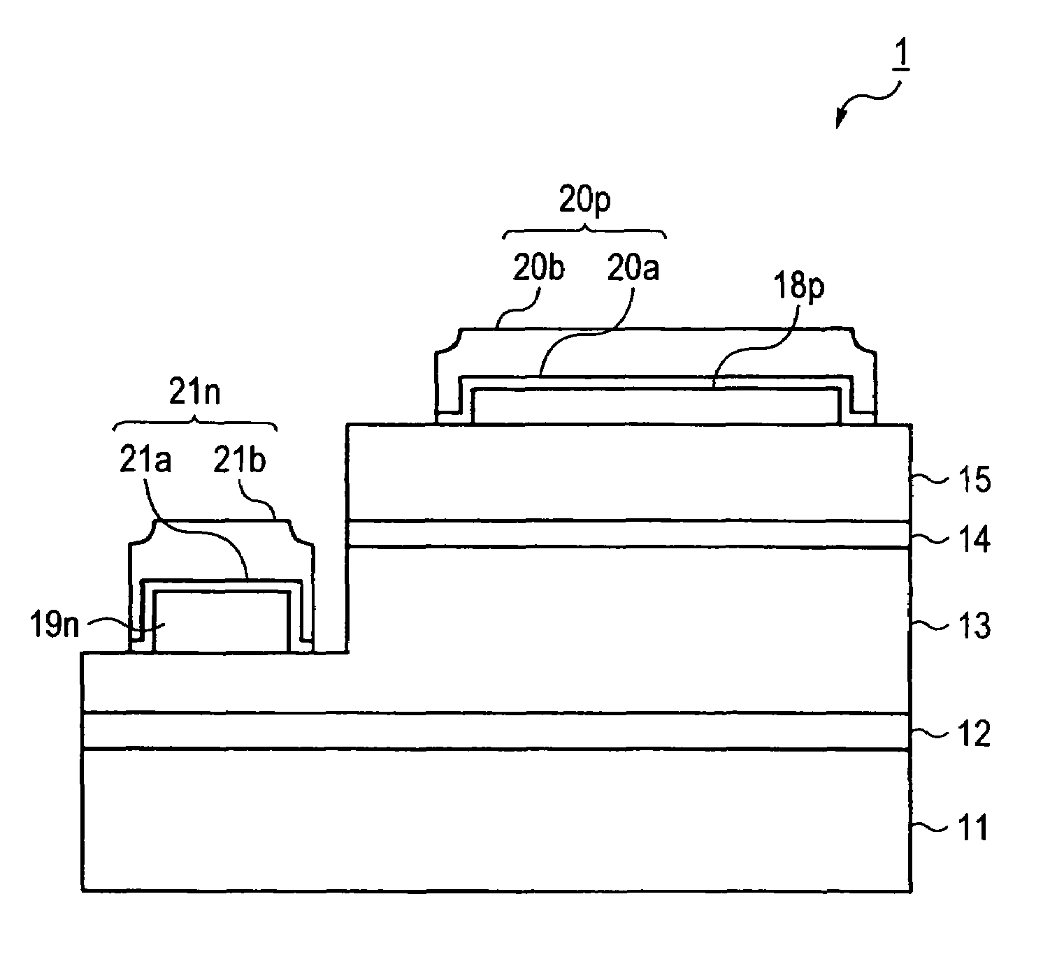
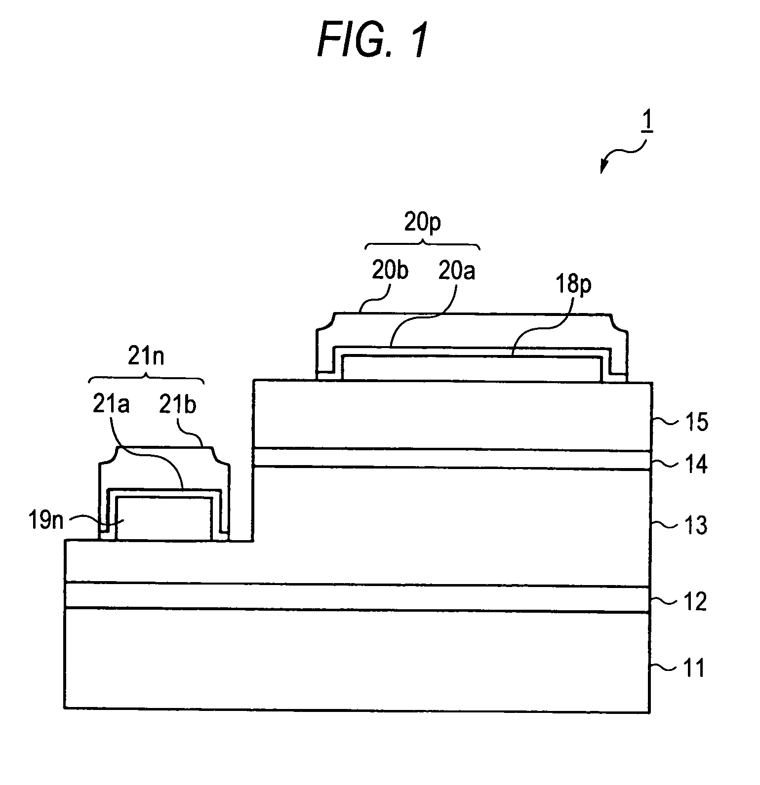
[0015]A Group III nitride compound semiconductor light-emitting element according to the invention is a flip chip type light-emitting element having a p-side electrode and an n-side electrode formed on one surface side. The flip chip type light-emitting element means a light-emitting element used in a flip chip type light-emitting device, that is, a light-emitting element which is used to be mounted on a support such as a board while the surface of the light-emitting element on which the p-side electrode and the n-side electrode are formed is used as a mount surface. Emitted light is radiated from the board side, that is, from a side opposite to the surface side on which the electrodes are formed.

[0016]The Group III nitride compound semiconductor light-emitting element means a light-emitting element having a light-emitting layer made of Group III nitride compound semiconductor. Here, the Group III nitride compound semiconductor is represented by the general formula AlXGaYIn1-X-YN (0...


PUM

PropertyMeasurementUnit
thicknessaaaaaaaaaa
thicknessaaaaaaaaaa
thicknessaaaaaaaaaa

Abstract

In a flip chip type Group III nitride compound semiconductor light-emitting element, an Au layer is provided on each of a surface of a p-side electrode and a surface of an n-side electrode with interposition of a Ti layer.

Description

REFERENCE TO PRIOR APPLICATION[0001]This application is the National Stage of International Application No. PCT / JP02 / 05430, filed on Jun. 3, 2002.TECHNICAL FIELD[0002]The present invention relates to a Group III nitride compound semiconductor light-emitting element. Particularly it relates to a Group III nitride compound semiconductor light-emitting element having a p-side electrode and an n-side electrode formed on one surface side and preferably used in a flip chip type light-emitting device.BACKGROUND ART[0003]There is known a (flip chip type) light-emitting device configured so that an element having a light-emitting layer of Group III nitride compound semiconductor is mounted on a support while a surface of the element on which a p-side electrode and an n-side electrode are formed is used as a mount surface. In this type light-emitting device, light emitted from the light-emitting layer of the light-emitting element passes through a light-transmissive substrate so as to be radi...

Claims


Application Information

Patent Timeline
Patent Type & Authority Patents(United States)
IPC IPC(8): H01L29/22H01L33/12H01L33/32H01L33/40H01L33/62
CPCH01L33/40H01L33/32H01L2924/181H01L2224/32257H01L2224/16145H01L2224/16225H01L2224/32245H01L2224/48091H01L2224/48247H01L2224/48465H01L2224/73265H01L2224/14H01L2224/05573H01L2224/05568H01L2224/05023H01L2224/05001H01L24/05H01L24/06H01L2224/0603H01L2224/06102H01L2224/1703H01L2924/00014H01L2924/00012H01L2924/00H01L2224/05644H01L2224/05111H01L2224/05124H01L2224/05139H01L2224/05144H01L2224/05147H01L2224/05155H01L2224/05164H01L2224/05166H01L2224/05169H01L2224/05171
Inventor UEMURA, TOSHIYAHORIUCHI, SHIGEMI
Owner TOYODA GOSEI CO LTD
Why Eureka
Try Eureka