
Eureka
For R&D, Eureka makes reading and utilizing patents & technical documents easy.
Eureka AIR
Designed for self-driven R&D workflows. Generate viable solutions, solve complex R&D challenges, empower your innovation with AI.

Eureka Materials
Designed for material experts only. Revolutionize your material R&D, from search, analyze, to developing new materials.

TechResearch
Generate reliable direction feasibility study reports for your R&D in just a few steps.

TechSeek
Discover and master advanced knowledge NOW. Basics, ideas, possibilities, all at once.

TechMind
As an expert in R&D Theories, TechMind can generates customized viable solutions instantly.

TechRisk
Analyze your overall solution with one click, know your potential R&D risks in advance.

TechMonitor
Get weekly tech updates, stay abreast of the latest tech innovations and key insights.
Plane emission type semiconductor laser device and method of manufacturing the same
- Summary
- Abstract
- Description
- Claims
- Application Information
AI Technical Summary
Benefits of technology
Problems solved by technology
Method used
Image

Examples
Embodiment Construction
[0073]Now, referring to the accompanying drawings, the present invention will be described more in detail below, based on embodiments thereof. The conduction type, kinds of films, film thicknesses, methods of forming films, sizes and the like are just examples for easy understanding of the present invention, and the invention is not limited to or by these examples.
Embodiment of Plane Emission Type Semiconductor Laser Device
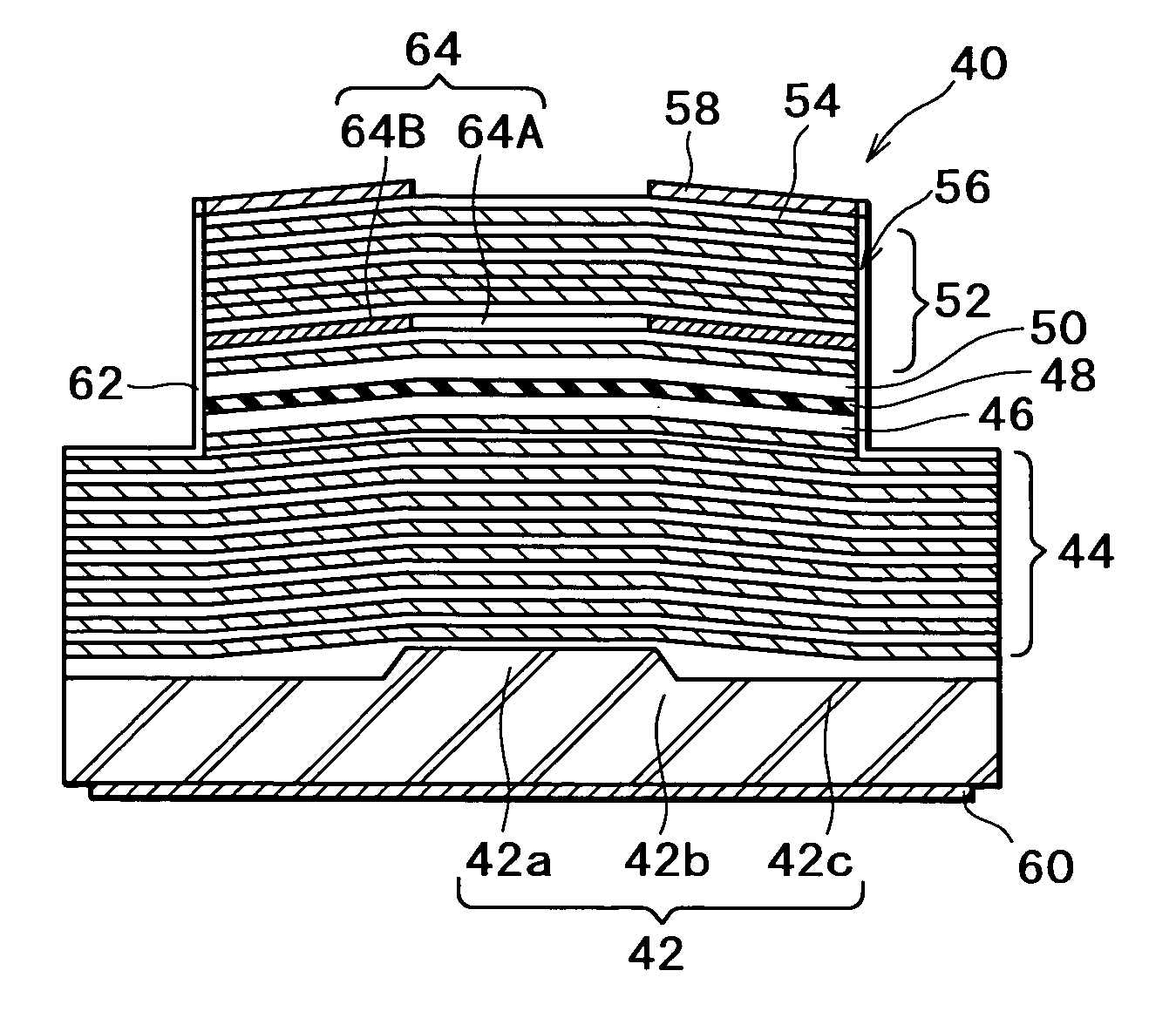
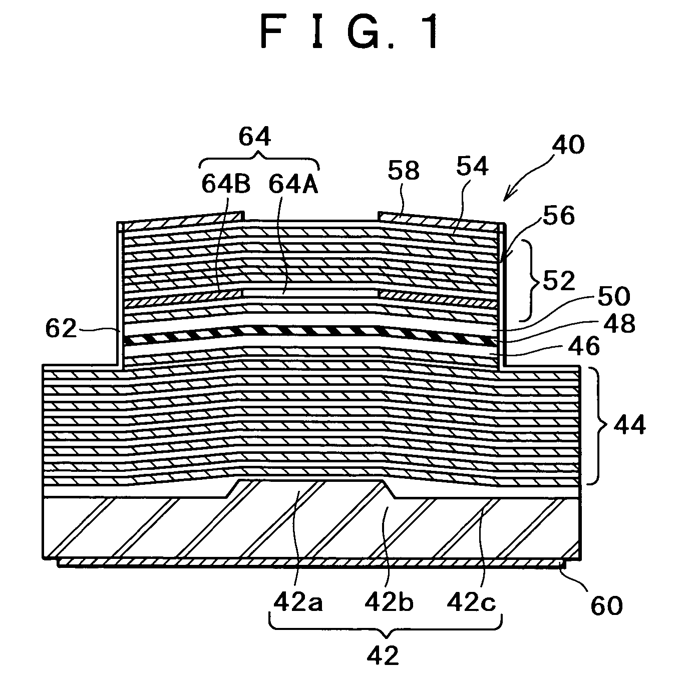
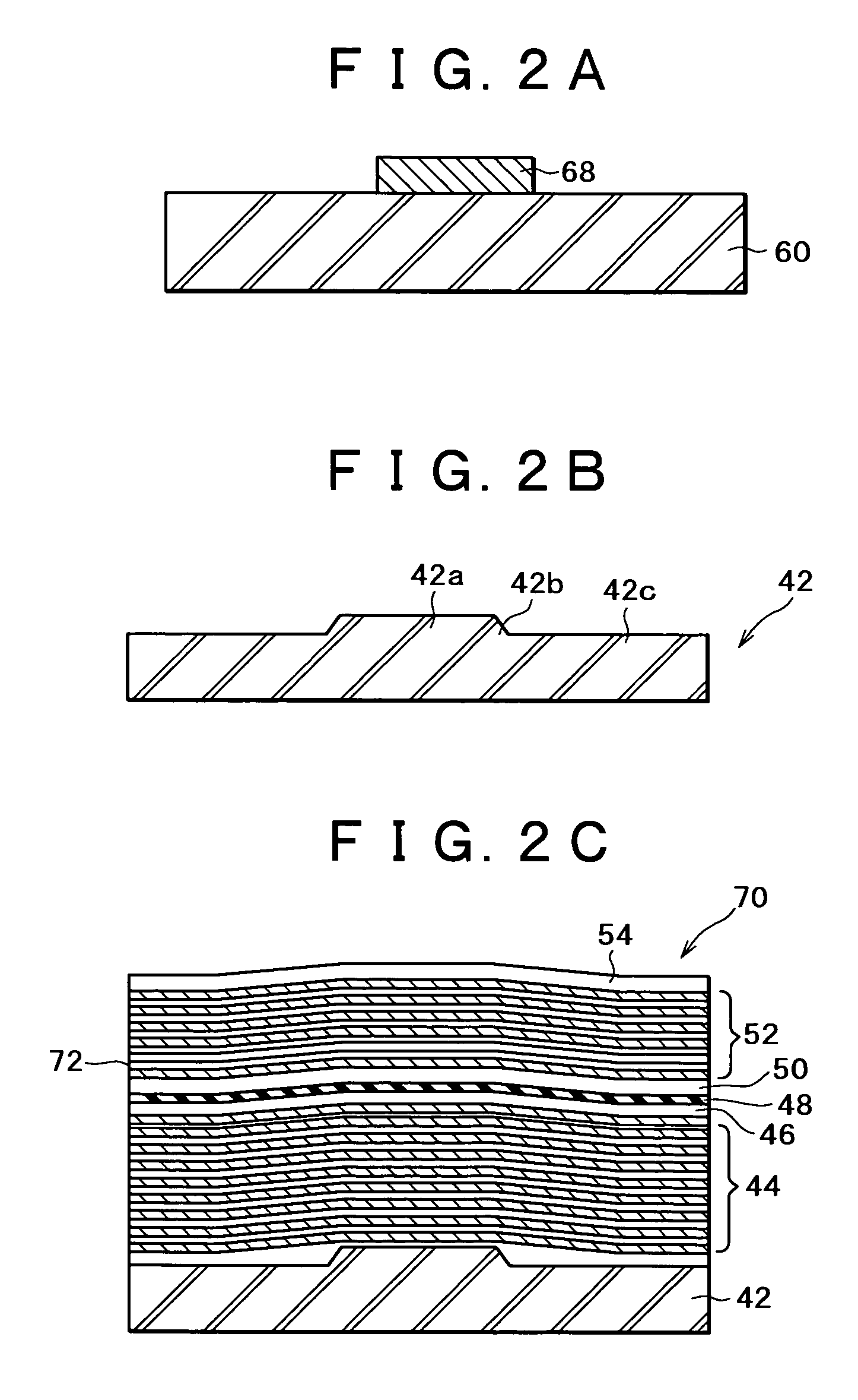
[0074]This embodiment is an example of embodiment of a plane emission type semiconductor laser device according to the present invention, and FIG. 1 is a sectional view showing the configuration of the plane emission type semiconductor laser device according to the embodiment.
[0075]The plane emission type semiconductor laser device 40 in this embodiment includes, on an n-type GaAs stepped substrate 42, a laminate structure of a lower reflector 44, a non-doped Al0.5Ga0.5As lower clad layer 46 with a film thickness of 100 nm, an active layer 48, a non-doped Al0.5Ga0...
PUM
 Abstract
Description
Claims
Application Information
 - R&D Engineer
- R&D Manager
- IP Professional
- Industry Leading Data Capabilities
- Powerful AI technology
- Patent DNA Extraction
Browse by: Latest US Patents, China's latest patents, Technical Efficacy Thesaurus, Application Domain, Technology Topic, Popular Technical Reports.
© 2024 PatSnap. All rights reserved.Legal|Privacy policy|Modern Slavery Act Transparency Statement|Sitemap|About US| Contact US: help@patsnap.com