Method for producing encapsulated chips

a technology of encapsulated chips and encapsulated chips, which is applied in the manufacturing of semiconductor/solid-state devices, solid-state devices, electric devices, etc., can solve the problems of preventing rapid introduction, requiring additional cost, and unable to build a system in packages in miniaturized implementation, so as to facilitate the stacking of several encapsulated chips on top of each other

Active Publication Date: 2006-03-14
FRAUNHOFER GESELLSCHAFT ZUR FOERDERUNG DER ANGEWANDTEN FORSCHUNG EV
View PDF17 Cites 20 Cited by
  • Summary
  • Abstract
  • Description
  • Claims
  • Application Information

AI Technical Summary

Benefits of technology

[0021]The present invention is based on the finding that enhanced redistribution may be achieved by dicing a wafer prior to the encapsulation and then subjecting the diced chips to injection molding. According to the invention, the wafer is disposed on the dicing substrate, so that the chips remain disposed on the dicing substrate both after dicing and during injection molding. With the inventive method, by the dicing of the chips prior to the encapsulation, the trenches between the chips are enabled to be filled with encapsulation material. Thereby, it may be achieved that an area of the chip unit formed after encapsulating, which includes the chip as well as a laterally disposed encapsulation mass, is larger than an area of the chip itself, so that an increased area is available for the encapsulated chip unit as compared to the chip. The extension of the existing area enables a redistribution of molded or encapsulated integrated circuits for the attainment of increased mean contact distances. The redistribution takes place in an inexpensive manner, since the additional area is provided by the cheap encapsulation material.
[0023]With the inventive method, also simplified handling with a high production rate is achieved, since the time-consuming arranging and transporting of diced chips is avoided by the wafer remaining arranged on the dicing substrate after dicing and during injection molding.
[0024]By using an injection molding method, the encapsulation method has reduced production costs with concurrent guarantee of a high production rate. For conducting, the injection molding method only requires the arranging of the chips and an injection molding part and then introducing the encapsulation material. Thereby, it has a high degree of automation and is particularly suited for methods in which a high production rate is required. Furthermore, the injection molding enables a concurrent shaping of functional structures of the encapsulated chips, so that they can be created in a simple and inexpensive way.
[0026]By the mechanical treatment, the area of the dicing substrate on which the chips are arranged increases, so that the chips are spaced from each other over a greater gap on the dicing substrate. Thereby, the area of a chip unit may easily be increased after encapsulating and adjusted to a predetermined value.
[0032]By introducing wires or pass-through conductors, 3D constructions may be realized, which allow a space-saving solution for the construction of multi-component systems. For example, the pass-through conductor may be used to enable an integrated via in a creation of a stackable system. The creation of the functional structures during the injection molding enables an even further simplification of a production of encapsulated chips in which such structures are required. For example, in one embodiment, the assembly of mechanical or optical functional units is facilitated by introduced microstructures in the encapsulation level. An optimized optical guide fiber adjustment may be achieved, for example, by direct realization of a V-notch in the encapsulation process or the geometric shaping of contact bumps which may be used for contacting the member by metalization and structurization of a redistribution layer.
[0036]Preferably, the injection molding is conducted such that the surface of the encapsulation material is planar with the surface of the projecting contacts. This enables that, in a subsequent redistribution, a planarizing of the surface is not required, so that the redistribution structure may be directly applied on the encapsulation material and the surface of the contacts as a thin layer. Furthermore, stacking of several encapsulated chips on top of each other is facilitated by creating a planar surface.

Problems solved by technology

It is disadvantageous about the prior-art procedures and methods that there is no possibility for the construction of a system in package in miniaturized implementation.
This is connected with additional cost, and also prevents quick introduction in the market.
This method has the disadvantage that, when creating an encapsulation layer on the entire wafer and subsequently dicing the wafer with the encapsulation layer, the diced chips units have an area that corresponds to the area of the chip.
Accordingly, with such a method, no redistribution beyond the area of the semiconductor chip is possible.
Furthermore, the method has the disadvantage that an encapsulation layer is only disposed on the main surface of the chips, with the side surfaces forming after the dicing not being encapsulated and therefore having a decreased mechanical protection.
Apart from the disadvantages already described above of encapsulating the entire wafer, this method also has the disadvantage of an expensive process sequence, in which first material is applied and then subjected to a melting procedure, wherein also mechanical actuation is required during molding.
This results in high production costs and a low production rate for the method.
Thereby, the expenses in the production thereof increase, so that production costs increase.
Furthermore, the use of a resin compression molding process is also disadvantageous for some applications.
Another disadvantage of the prior art is that the integration of functional structures on the encapsulation level is not provided.

Method used


Image

  • Method for producing encapsulated chips
  • Method for producing encapsulated chips
  • Method for producing encapsulated chips

Examples


Embodiment Construction

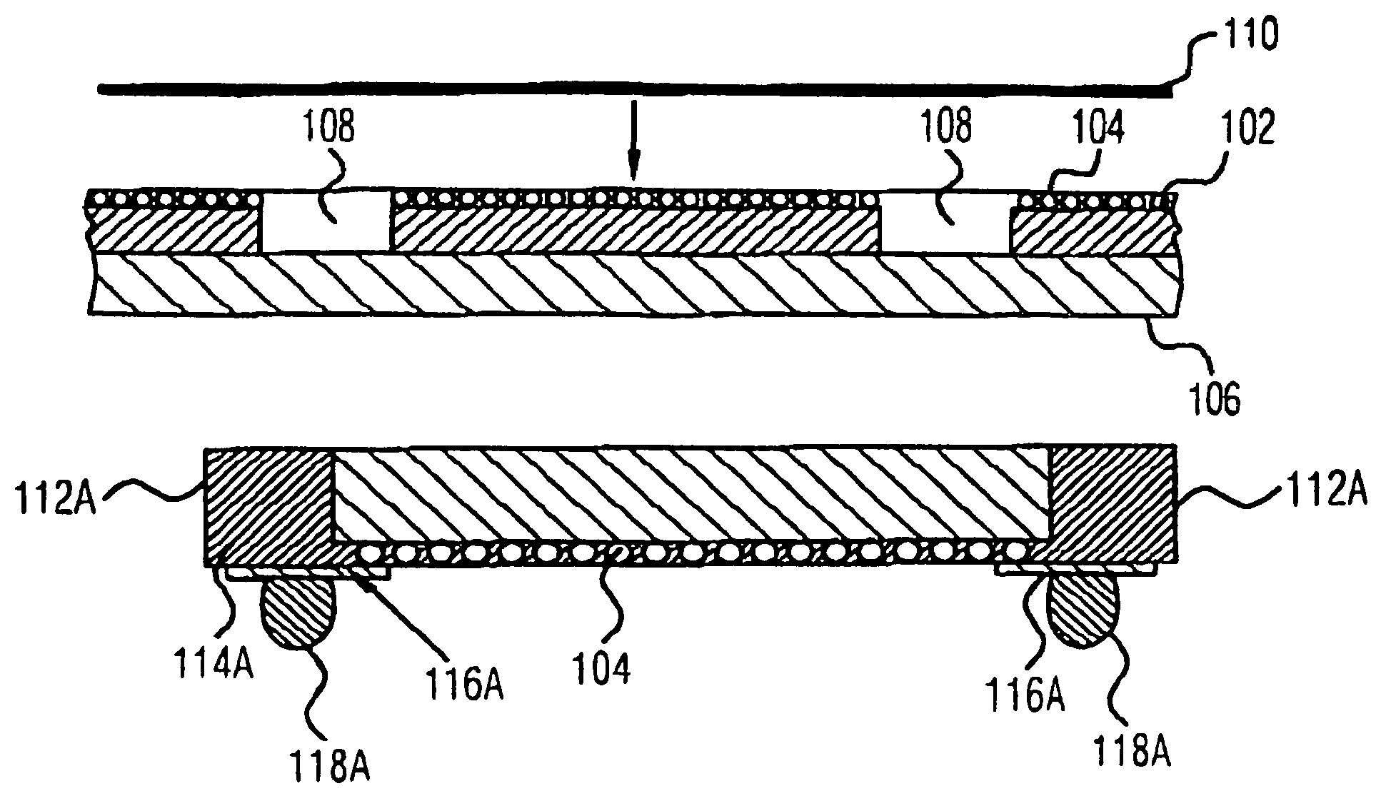
[0047]In the following, with reference to FIGS. 3a–c and FIGS. 4a–f, a first embodiment of a single-stage wafer-level encapsulation according to the present invention is explained, which also allows to process hybrid systems constructed on wafer level, which may include different chip types, mechanical functional units, MEMS, or MOEMS. FIGS. 3a–c show various phases during dicing a wafer 100, and FIGS. 4a–f show various phases during encapsulation by means of injection molding. In the various figures of the following embodiments, similar elements are provided with similar reference numerals, respectively.

[0048]FIG. 3a shows a wafer 100 that has been prepared so that it includes a plurality of chips 102. The chips 102 include functional units, such as integrated circuits, sensors or sensor structures, mechanical or optical functional units, such as MEMS (micro-electromechanical systems) or MOEMS (micro-optical-electromechanical structures), which are arranged on a surface 100a, for e...


PUM


Abstract

A method for producing encapsulated chips includes preparing a wafer with contacts projecting from a surface of the wafer. The wafer is disposed on a dicing substrate and diced into a plurality of spaced chips on the dicing substrate. The contacts are covered with a protection arrangement, then injection molding being conducted to introduce encapsulation material into the contacts and the trenches. Then the protection arrangement is removed so that the contacts are exposed.

Description

BACKGROUND OF THE INVENTION[0001]1. Field of the Invention[0002]The present invention relates to the encapsulating of semiconductor structures and, in particular, to the producing of encapsulated chips.[0003]2. Description of the Related Art[0004]As it is known, for wafer-level encapsulation, methods are employed to mechanically stabilize wired integrated circuits, to protect the active structures and to achieve the easy construction of high bumps. In a commercially available implementation, with the increasing integration density and compactness of the semiconductor structures, it is being aimed at a wafer-level encapsulation of single integrated circuits with a fan-in redistribution in the range of mean contact distances greater than 400 μm.[0005]FIG. 1 schematically shows depictions illustrating a method in which a wafer 10 with chips disposed thereon is first encapsulated and the encapsulated wafer 10 is then severed along separating lines 12 for producing diced chips 14. As can...

Claims


Application Information

Patent Timeline
Patent Type & Authority Patents(United States)
IPC IPC(8): H01L21/44H01L21/56H01L21/60H01L21/68H01L21/78H01L23/31H01L23/538H01L25/10
CPCH01L21/56H01L24/27H01L21/568H01L21/6835H01L21/6836H01L21/78H01L23/3107H01L23/5389H01L24/18H01L24/82H01L24/97H01L25/105H01L21/561H01L2221/68327H01L2224/13111H01L2224/13147H01L2224/16H01L2224/18H01L2224/274H01L2224/97H01L2924/01013H01L2924/01029H01L2924/01082H01L2924/01322H01L2924/10329H01L2924/14H01L2924/15173H01L2924/18161H01L2924/19104H01L2225/1058H01L2924/01005H01L2924/01006H01L2924/01023H01L2924/01033H01L2924/014H01L2225/1035H01L2224/82H01L24/19H01L24/96H01L2224/04105H01L2224/12105H01L2924/18162H01L2924/181H01L2924/12042H01L2224/2518H01L2924/00
Inventor BECKER, KARL-FRIEDRICHBRAUN, TANJAKOCH, MATHIASOSTMANN, ANDREASBOTTCHER, LARSJUNG, ERIK
Owner FRAUNHOFER GESELLSCHAFT ZUR FOERDERUNG DER ANGEWANDTEN FORSCHUNG EV
Why Eureka
Try Eureka