System chip synthesis

Inactive Publication Date: 2006-03-14
CADENCE DESIGN SYST INC
View PDF14 Cites 55 Cited by
  • Summary
  • Abstract
  • Description
  • Claims
  • Application Information

AI Technical Summary

Benefits of technology

[0018]In general, the present invention is new methodology for the design and implementation of deep sub-micron integrated circuits, in which the delays of the global wires are minimized first, before the logic is synthesized and optimized. This results

Problems solved by technology

The NTRS report concluded that the industry is rapidly approaching a formidable “100 nm barrier” that threatens the continuation of the historical success the industry has enjoyed.
The most alarming finding of this working group was that the industry has become very “idea limited,” and almost all areas of design technology would hit a brick wall by the year 2006, when the industry anticipates the first shipment of 100 nm technology.
However, it has become very clear that even if the various components of a design automation toolset could handle specific issues in their respective domain, the overall problems of size, diversity and productivity may not he solved unless a coherent and comprehensive approach to tools working together in a convergent flow is taken.
Also, for “deep sub-micron” (DSM) manufacturing processes (i.e. those less than or equal to 0.18 micron), the problem of wire delay becomes a significant issue.
Prior t

Method used


Image

  • System chip synthesis
  • System chip synthesis
  • System chip synthesis

Examples


Embodiment Construction

[0038]The following description is provided to enable any person skilled in the art to make and use the invention and sets forth the best modes contemplated by the inventor for carrying out the invention. Various modifications, however, will remain readily apparent to those skilled in the art, since the basic principles of the present invention have been defined herein specifically to provide a method for designing and implementing deep sub-micron integrated circuits. Any and all such modifications, equivalents and alternatives are intended to fall within the spirit and scope of the present invention.

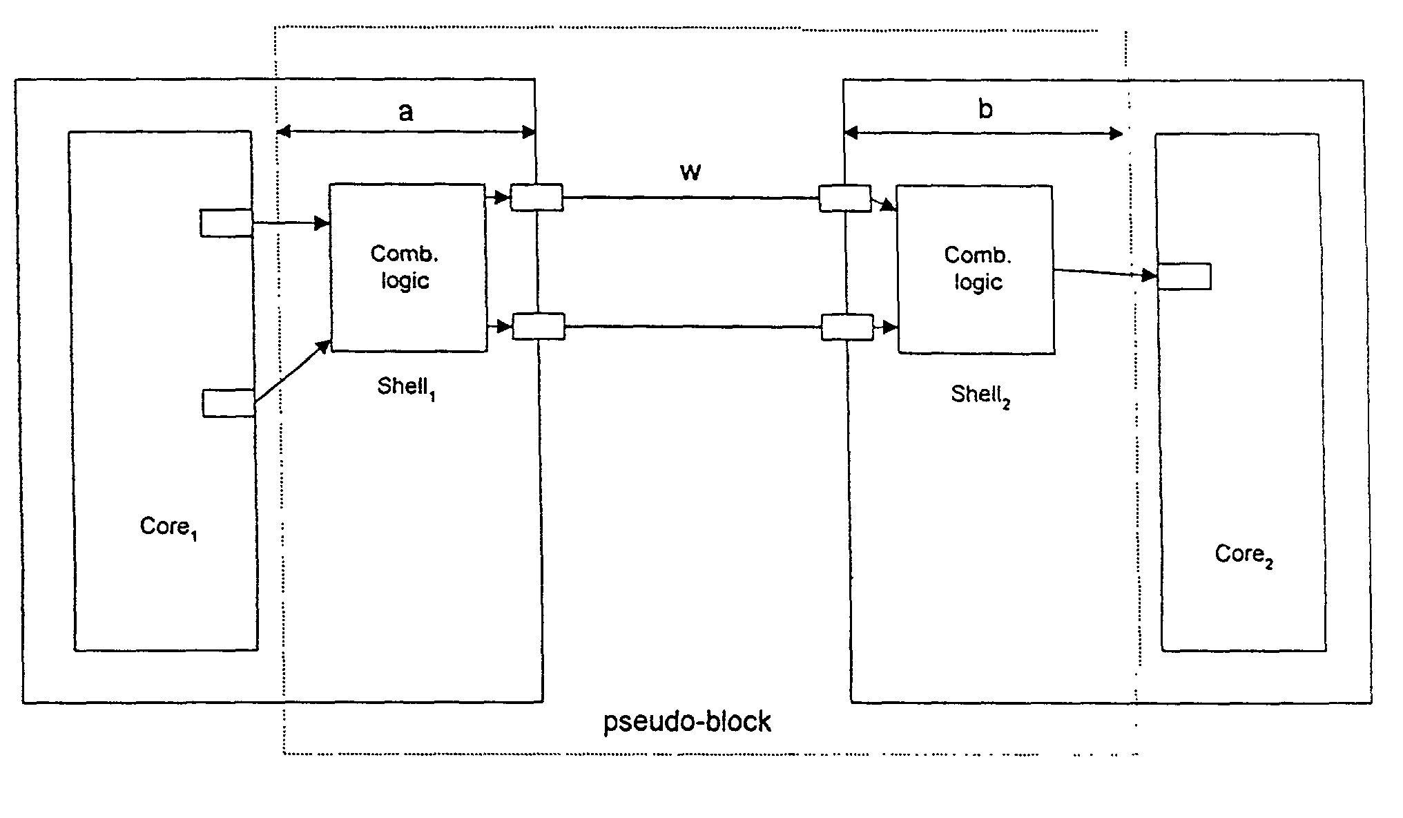
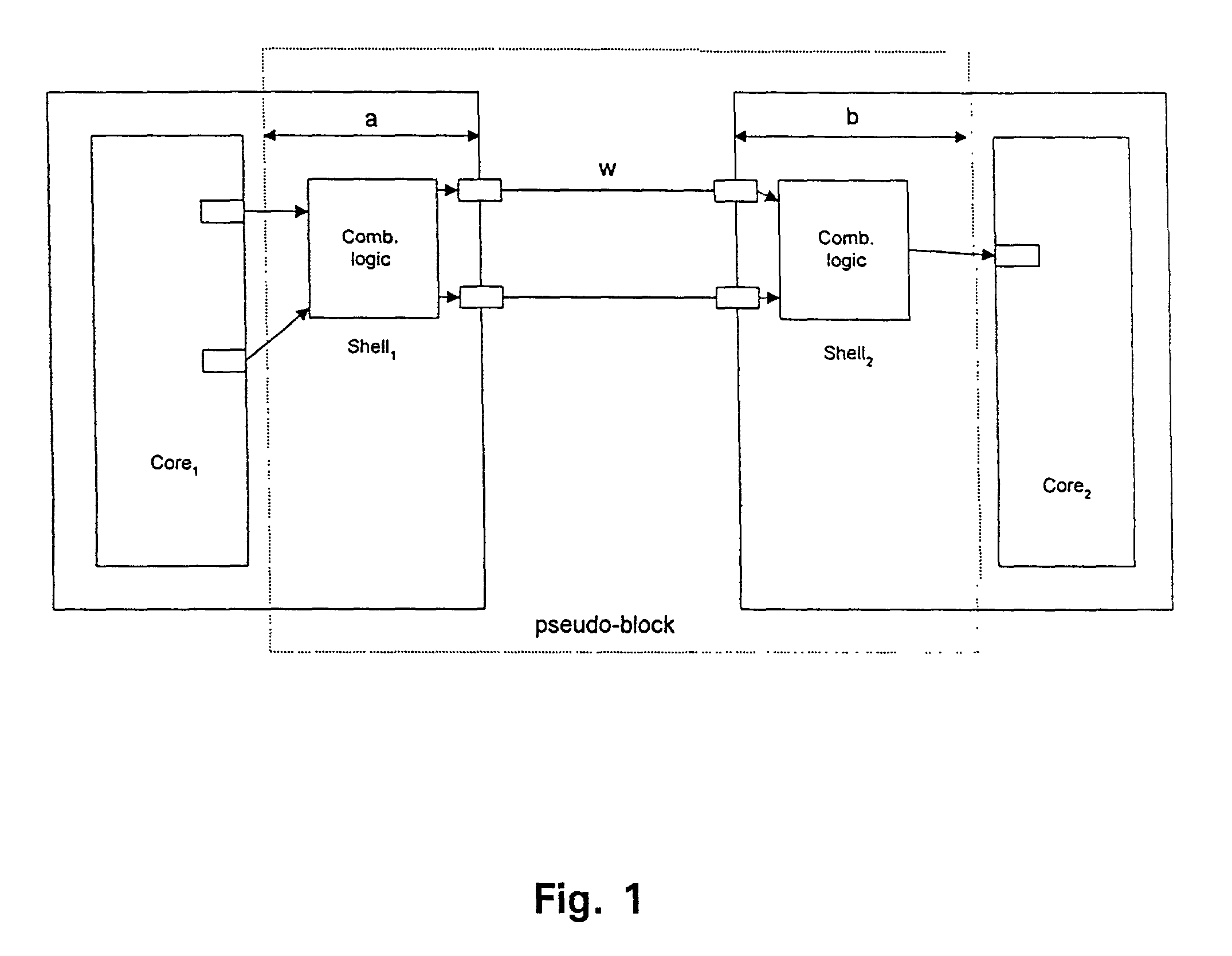
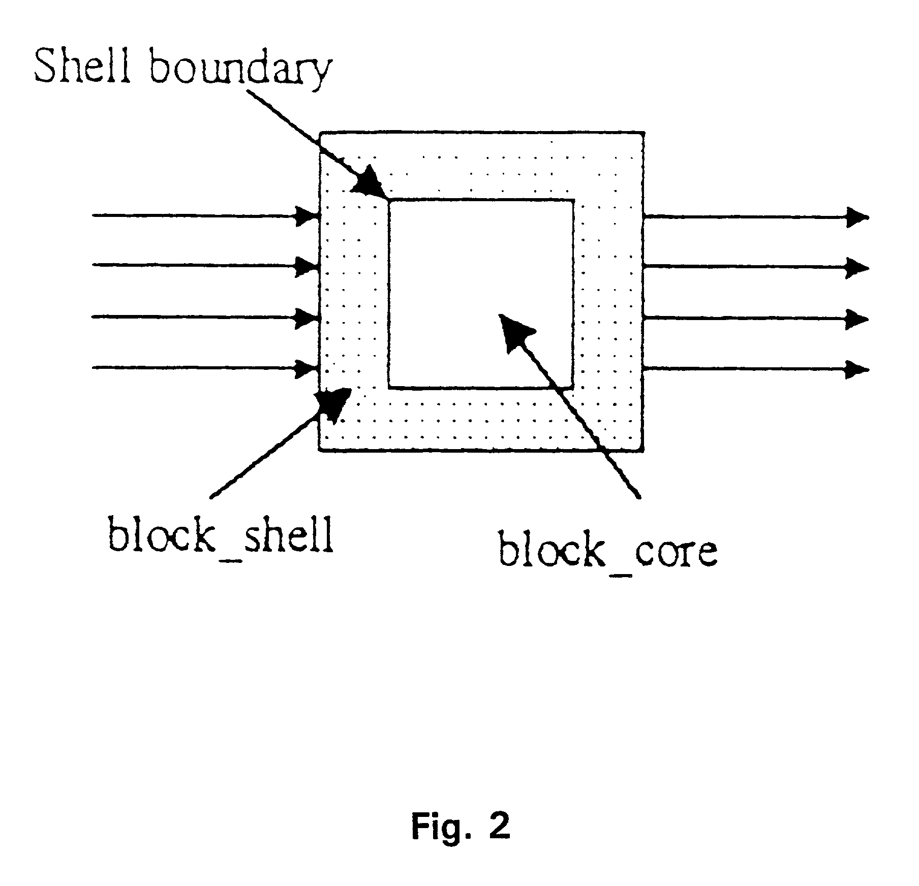
[0039]In general, the present invention is new methodology for the design and implementation of deep sub-micron integrated circuits, in which the delays of the global wires are minimized first, before the logic is synthesized and optimized. This results in a substantial improvement in productivity and convergence of complex deep sub-micron systems on a chip. The present invention reduce...


PUM


Abstract

A technique to design deep sub-micron (DSM) integrated circuits is disclosed, in which global wire delays are minimized first, before performing logic synthesis. According to the present method, a designer performs layout of physical blocks by estimating an area for each block. After connecting the pins of the blocks with no timing constraints, each wire is assigned to a metal layer, based on length. The delay of each wire is minimized by inserting buffers at optimal distances. The blocks are then partitioned into “cores” and “shells.” The shells and cores are synthesized, and then recombined. This procedure greatly reduces the number of design iterations required to complete a design.

Description

CROSS REFERENCE TO RELATED APPLICATIONS AND CLAIM OF PRIORITY[0001]This application claims priority to U.S. Provisional Application Ser. No. 60 / 245,334 entitled “SYSTEM CHIP SYNTHESIS,” filed Nov. 1, 2000, the contents of which are incorporated herein by reference in their entirety. Furthermore, this application is related to U.S. patent application Ser. No. 09 / 919,740, entitled “INSERTION OF REPEATER WITHOUT TIMING CONSTRAINT” filed Aug. 1, 2001, the contents of which are incorporated herein by reference in their entirety.COPYRIGHT NOTICE[0002]A portion of the disclosure of this patent document contains material which is subject to copyright protection. The copyright owner has no objection to the facsimile reproduction by anyone of the patent document or the patent disclosure, as it appears in the Patent and Trademark Office patent file or records, but otherwise reserves all copyright rights whatsoever.BACKGROUND OF THE INVENTION[0003]1. Field of Invention[0004]The present inventio...

Claims


Application Information

Patent Timeline
IPC IPC(8): G06F17/50
CPCG06F17/505G06F30/327
Inventor SALDANHA, ALEXANDERHIGGINS, JOEMEHROTRA, AMIT
Owner CADENCE DESIGN SYST INC
Why Eureka
Try Eureka