High power flip chip LED

a high-power flip and chip technology, applied in the direction of electrical equipment, semiconductor devices, semiconductor/solid-state device details, etc., can solve the problems of uniform current density across leds, uniform emission, and structure failure to solve uniformity sufficiently, so as to achieve high power flip, increase luminous area, and high brightness light

Inactive Publication Date: 2006-03-21
SAMSUNG ELECTRONICS CO LTD
View PDF2 Cites 58 Cited by
  • Summary
  • Abstract
  • Description
  • Claims
  • Application Information

AI Technical Summary

Benefits of technology

[0012]The present invention has been made to solve the foregoing problems and it is therefore an object of the present invention to provide a high power flip chip LED which can prevent the current channeling to increase the luminous area while equalizing the current density across the luminous area thereby generating high brightness light.

Problems solved by technology

This makes the current density across the LED ununiform and also the emission ununiform.
However, this structure also fails to sufficiently solve the ununiformity of the current density across the LED.

Method used


Image

  • High power flip chip LED
  • High power flip chip LED
  • High power flip chip LED

Examples


first embodiment

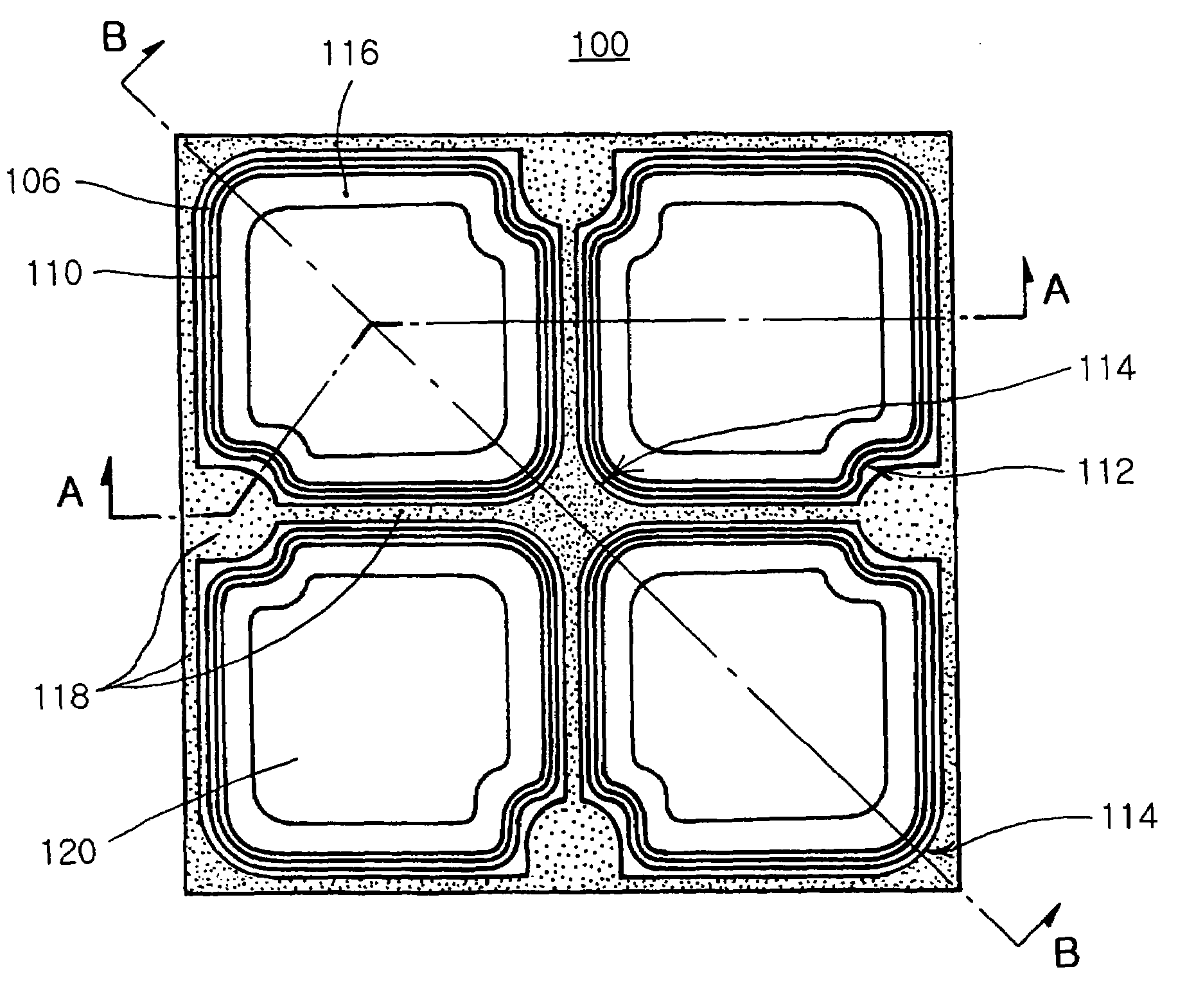
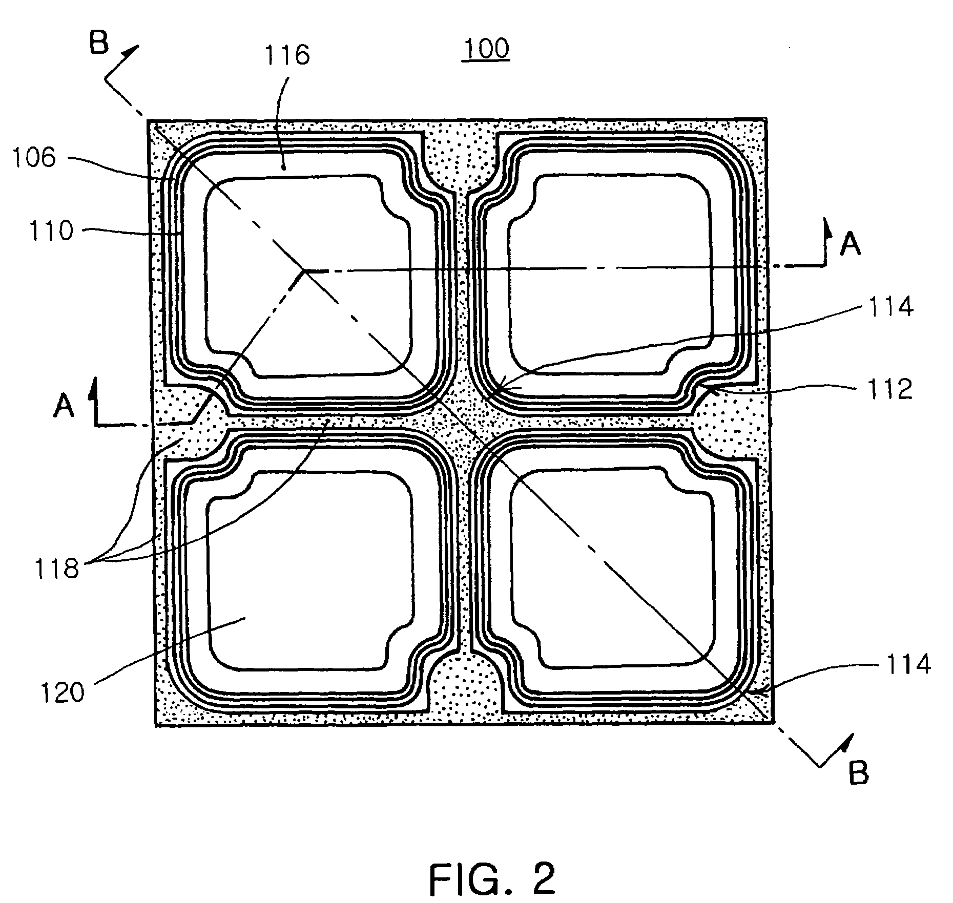
[0033]FIG. 2 is a plan view illustrating a flip chip LED according to the invention, FIG. 3 is a sectional view taken along a line A—A in FIG. 2, and FIG. 4 is a sectional view taken along a line B—B in FIG. 2.

[0034]Referring to FIGS. 2 to 4, a flip chip LED 100 according to the first embodiment of the invention includes a substantially rectangular substrate 102, an n-doped semiconductor layer 104 formed on the substrate 102, a plurality of p-doped semiconductor layers 110 formed on first regions 106 of the n-doped semiconductor layer 104, a plurality of first metal layers 116 formed on the p-doped semiconductor layers 110, separated from one another, a second metal layer 118 formed on the second region 108 of the n-doped semiconductor layer 104, a plurality of p-contacts 120 formed respectively on the first metal layers 116 and a plurality of n-contacts formed in predetermined positions on the second metal layer 118 (corresponding to first basins 112).

[0035]The rectangular substrat...

third embodiment

[0052]In the LED 300 of the third embodiment, the n-contacts are placed at four corners of p-contacts. That is, each mesa structure is rounded inward with its four corners to form basins 312 for containing the n-contacts of a second metal layer 318. Therefore, since each first metal layer 316 is configured symmetric about the n-contacts and placed more adjacent to the n-contacts, carriers (i.e., electrons) from the second metal layer 318 more uniformly flow in active regions, i.e., light emitting regions between first regions 306 of an n-doped semiconductor layer and p-doped semiconductor layers 310.

[0053]FIG. 7 is a plan view illustrating a flip chip LED according to a fourth embodiment of the invention. Referring to FIG. 7, an LED 400 of the fourth embodiment has a combined configuration of the LED 100 of the first embodiment and the LED 200 of the second embodiment. That is, first basins 412 are formed at the side of a pair of diagonal corners of a pair of mesa structures, and se...


PUM


Abstract

A high power flip chip LED has an n-doped semiconductor layer formed on the sapphire substrate, with a plurality of first regions and a second region of intersecting lines for separating the first regions from each other. P-doped semiconductor layers are on the first regions of the n-doped semiconductor layer to form mesa structures. At least one pair of diagonal corners of the respective mesa structures are rounded inward to form first basins between adjacent inward-rounded corners. First metal layers are on the mesa structures in a same configuration. A second metal layer is on the second region of the n-doped semiconductor layer. First ohmic contacts are on the first metal layers. Second ohmic contacts are on the second metal layer in the first basins. The LED can prevent the current channeling to increase the luminous area while equalizing the current density area thereby generating high brightness light.

Description

BACKGROUND OF THE INVENTION[0001]1. Field of the Invention[0002]The present invention relates to a high power flip chip LED, more particularly, which can prevent the current channeling to increase the luminous area while equalizing the current density across the luminous area thereby generating high brightness light.[0003]2. Description of the Related Art[0004]A Light Emitting Diode (LED) basically consists of a junction of p- and n-doped semiconductor layers formed on a sapphire substrate as a kind of optoelectric device. When applied with electric current, the LED generates light converted from a predetermined level of energy corresponding to its band gap through the electron-hole re-combination.[0005]People have become familiar with LEDs of this type as they are adopted in displays of general electronic instruments. Although early stage LEDs were limited in the brightness and color, various high brightness LEDs are produced at present according to advanced materials and improved ...

Claims


Application Information

Patent Timeline
Patent Type & Authority Patents(United States)
IPC IPC(8): H01L33/00H01L27/15H01L29/08H01L33/06H01L33/10H01L33/20H01L33/32H01L33/40H01L33/62
CPCH01L27/156H01L33/08H01L2224/0603
Inventor PARK, YOUNG HOHAHM, HUN JOOYOO, SEUNG JIN
Owner SAMSUNG ELECTRONICS CO LTD
Why Eureka
Try Eureka