Reinforced solder bump structure and method for forming a reinforced solder bump

a solder bump and reinforced technology, applied in the field of solder connection, can solve the problems of increasing ic chip processing speed and ic chip pin count, new improved technology for fine-pitch wire bonding structure cannot keep pace with demand, and substantially impair device reliability

Inactive Publication Date: 2006-03-21
SAMSUNG ELECTRONICS CO LTD
View PDF34 Cites 117 Cited by
  • Summary
  • Abstract
  • Description
  • Claims
  • Application Information

AI Technical Summary

Problems solved by technology

New improved technologies for achieving fine-pitch wire bonding structures cannot keep pace with the demand resulting from increased IC chip processing speeds and higher IC chip pin counts.
Mechanical stresses on the solder bump are a source of structural defects and related failures which can substantially impair device reliability.
Conversely, when the chip cools during an idle state, both the chip and the PCB substrate contract in size.
The chip and the PCB substrate, however, have mismatched coefficients of thermal expansion, and therefore expand and contract at different rates, thus placing mechanical stress on the intervening solder bumps. FIG. 3 illustrates an example in which mechanical stresses have caused a substantially horizontal crack to form and begin propagating through the solder bump.
The larger the crack, the more the interconnection becomes degraded or impaired, and device failures, particularly soft failures, can begin arising even before the cracks propagate completely through the solder bump structure.

Method used


Image

  • Reinforced solder bump structure and method for forming a reinforced solder bump
  • Reinforced solder bump structure and method for forming a reinforced solder bump
  • Reinforced solder bump structure and method for forming a reinforced solder bump

Examples


first exemplary embodiment

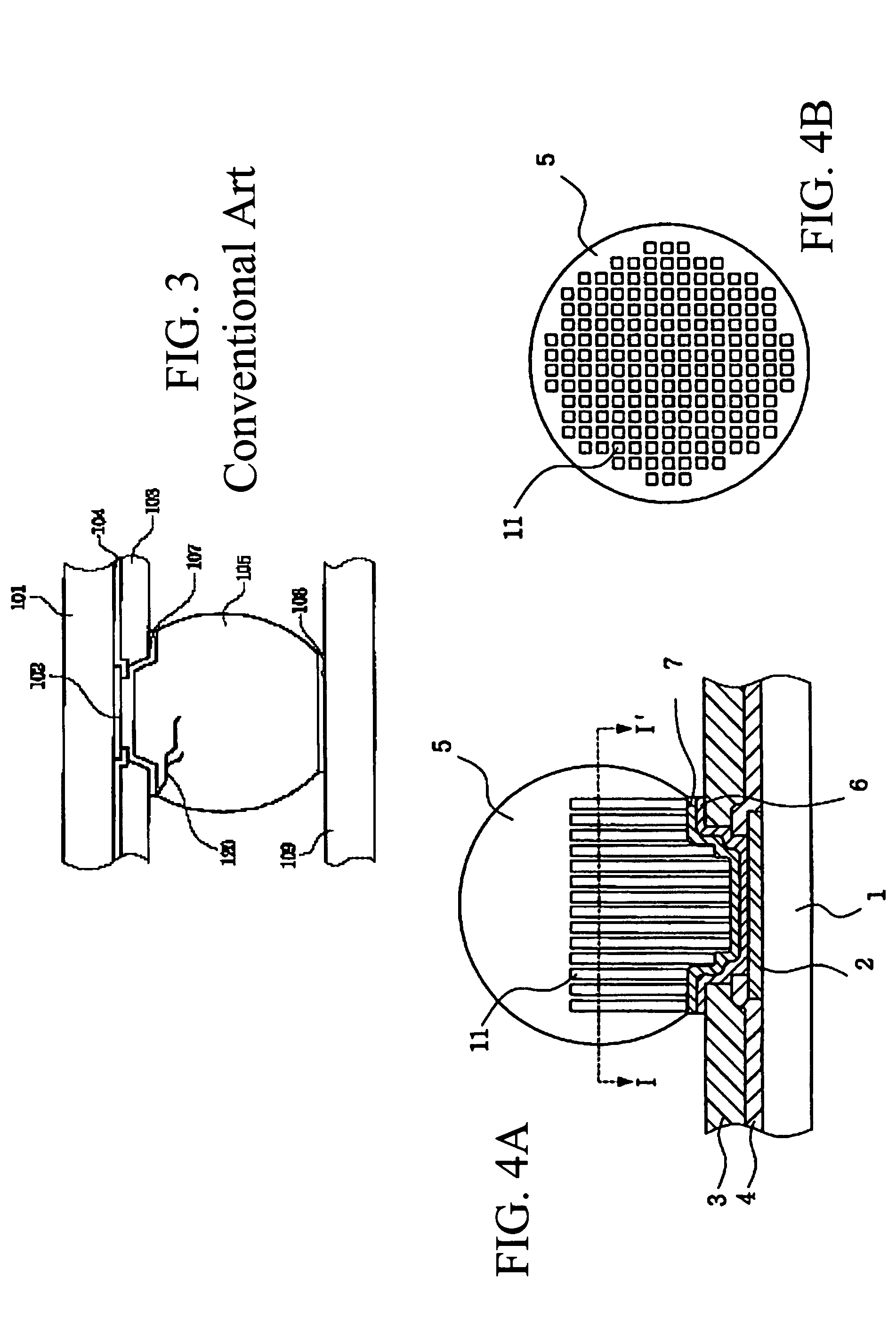
[0037]A first exemplary embodiment of a solder bump connector according to the present invention is illustrated in FIGS. 5A–B with FIG. 5A illustrating a vertical cross-section through an exemplary solder bump connector and FIG. 5B illustrating a horizontal cross-section through the reinforcing protrusions extending from the mounting substrate along a plane passing through line I–I′. The solder bump connector structure includes a contact pad 102 of an electronic device such as a semiconductor chip 101 intended for use in a flip chip package or a wafer level package. An opening is defined in one or more passivation layers 103, 104 to expose a surface of the chip pad 102. Interposed between the solder bump connector 105 and the chip pad 102 may be one or more intermediate or barrier layers 106, 107. The intermediate layers 106, 107 may be under bump metallurgy (UBM) layers in which, for example, the lower layer 106 may be a UBM adhesion layer comprising Cr, Ni or TiW, and the upper la...

second exemplary embodiment

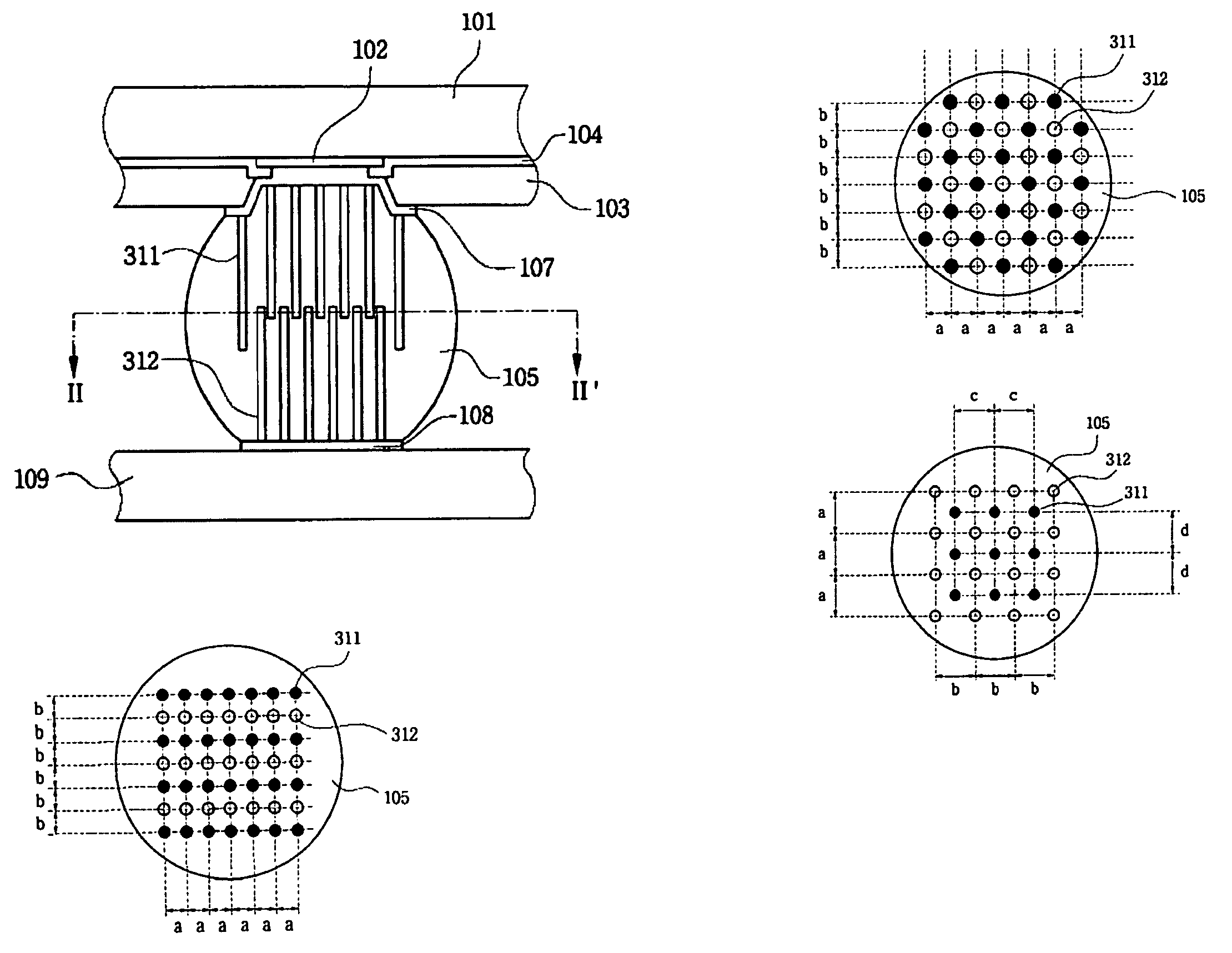
[0043]A second exemplary embodiment of a solder bump connector according to the present invention is illustrated in FIGS. 6A–D with FIG. 6A illustrating a vertical cross-section through an exemplary solder bump connector and FIGS. 6B–D illustrating a horizontal cross-sections through various configurations of the reinforcing protrusions extending from the mounting substrate along a plane passing through line II–II′. As illustrated and described with regard to FIG. 5A, the solder bump connector structure of FIG. 6A includes a contact pad 102 of an electronic device such as a semiconductor chip 101 intended for use in a flip chip package or a wafer level package. An opening is defined in one or more passivation layers 103, 104 to expose a surface of the chip pad 102. Interposed between the solder bump connector 105 and the chip pad 102 may be one or more intermediate or barrier layers 106, 107. The intermediate layers 106, 107 may be under bump metallurgy (UBM) layers in which, for ex...

third exemplary embodiment

[0050]A third exemplary embodiment of a solder bump connector according to the present invention is illustrated in FIGS. 7A–C with FIG. 7A illustrating a vertical cross-section through an exemplary solder bump connector, FIG. 7B providing an orthogonal view of the separated semiconductor chip 101 and mounting substrate 109, and FIG. 7C illustrating a horizontal cross-sections through the configuration of the reinforcing protrusions extending from the mounting substrate along a plane passing through line II–II′ of FIG. 7A. As illustrated and described with regard to FIG. 6A, the solder bump connector structure of FIG. 7A includes a contact pad 102 of an electronic device such as a semiconductor chip 101 intended for use in a flip chip package or a wafer level package. An opening is defined in one or more passivation layers 103, 104 to expose a surface of the chip pad 102. Interposed between the solder bump connector 105 and the chip pad 102 may be one or more intermediate or barrier ...


PUM


Abstract

A reinforced solder bump connector structure is formed between a contact pad arranged on a semiconductor chip and a ball pad arranged on a mounting substrate. The semiconductor chip includes at least one reinforcing protrusion extending upwardly from a surface of an intermediate layer. The mounting substrate includes at least one reinforcing protrusion extending upwardly from a ball pad, the protrusions from both the chip and the substrate being embedded within the solder bump connector. In some configurations, the reinforcing protrusion from the contact pad and the ball pad are sized and arranged to have overlapping under portions. These overlapping portions may assume a wide variety of configurations that allow the protrusions to overlap without contacting each other including pin arrays and combinations of surrounding and surrounded elements. In each configuration, the reinforcing protrusions will tend to suppress crack formation and / or crack propagation thereby improving reliability.

Description

CROSS-REFERENCE TO RELATED APPLICATIONS[0001]This application is a continuation-in-part of U.S. patent application Ser. No. 10 / 339,456, filed Jan. 10, 2003, and claims priority from Korean Application No. 2003-65946, filed Sep. 23, 2003, the contents of which are incorporated herein by reference in their entirety.BACKGROUND OF THE INVENTION[0002]1. Field of the Invention[0003]The present invention generally relates to solder connections useful for integrated circuit (IC) chips and devices and, more particularly, to reinforced solder bump structures that reduce mechanical failures of IC chips and devices, and to exemplary methods for forming such solder bump structures.[0004]2. Description of the Related Art[0005]As integrated circuits (IC's) advance toward higher speeds and larger pin counts, first-level interconnection techniques employing wire bonding technologies have approached or even reached their limits. New improved technologies for achieving fine-pitch wire bonding structur...

Claims


Application Information

Patent Timeline
Patent Type & Authority Patents(United States)
IPC IPC(8): H01L21/461H01L21/469H01L21/60B23K3/06H01L23/485H05K1/11H05K3/24H05K3/34
CPCB23K3/0607B23K3/0623H01L21/2885H01L21/4853H01L23/49811H01L24/03H01L24/05H01L24/11H01L24/16H01L24/81H05K1/111H05K3/3436H01L24/13H01L2224/0401H01L2224/05599H01L2224/1147H01L2224/11901H01L2224/13012H01L2224/13099H01L2224/13111H01L2224/13144H01L2224/13147H01L2224/16H01L2224/81143H01L2224/81193H01L2224/8121H01L2224/81815H01L2924/01002H01L2924/01004H01L2924/01005H01L2924/01006H01L2924/01013H01L2924/01015H01L2924/01022H01L2924/01028H01L2924/01029H01L2924/01033H01L2924/01046H01L2924/01047H01L2924/0105H01L2924/01078H01L2924/01079H01L2924/01082H01L2924/01327H01L2924/014H01L2924/14H05K3/243H05K3/4007H05K2201/0367H05K2201/0373H05K2201/09745H05K2201/10674H05K2203/048H05K2203/167H01L2924/01024H01L2924/01068H01L2224/136H01L2224/1601H01L2924/00014H01L2224/81141H01L2224/13076H01L2224/13078H01L2924/12042Y02P70/50H01L2924/00
Inventor JEONG, SE-YOUNGKIM, NAM-SEOGYONG, OH-SEKIM, SOON-BUMPARK, SUN-YOUNGLYU, JU-HYUNLEE, IN-YOUNG
Owner SAMSUNG ELECTRONICS CO LTD
Why Eureka
Try Eureka