Sigma-delta converter with noise suppression

a converter and delta technology, applied in the field of delta converters, can solve the problems of destructive overlaid noise components of the two paths

Inactive Publication Date: 2006-03-21
NOKIA SIEMENS NETWORKS GMBH & CO KG
View PDF10 Cites 9 Cited by
  • Summary
  • Abstract
  • Description
  • Claims
  • Application Information

AI Technical Summary

Benefits of technology

[0017]The spectral shaping of the input signal x(k) in accordance with the transmission function of the sigma-delta modulator in the principal path and the subsequent differential formation with the digital output signal of the sigma-delta modulator essentially isolates the quantization errors of the sigma-delta modulator in the principal path. The subsequent filtering then attenuates the noise components outside the useful band which represent the fundamental components of the noise power. This structure of a sigma-delta converter overlays the signal components of the principal and parallel paths constructively, while the noise components of the two paths are overlaid destructively. As a result, the quantization noise of the sigma-delta converters can be compensated for at least partly. This parallel circuit functions without feedback paths.
[0019]If the fundamental components of the noise power are suppressed, the amplitude of the signal can be increased without the sigma-delta modulator being overdriven.
[0022]In a development of the invention, the principal path is configured in such a way that compensation filtering is provided after the branch to the parallel path and before the digital to analog conversion. The compensation filtering in the principal path can compensate for the propagation times and the frequency responses in the parallel path which contains a filter, an amplifier and a sigma-delta converter. This additional filter can compensate for error components in the parallel path.
[0023]The sigma-delta converter in the principal path is advantageously configured as a multi-stage sigma-delta converter. In multi-stage sigma-delta converters, the principle of the onward transfer of the quantization noise can be exploited with the result that the quantization noise of the individual stages is overlaid destructively, that is to say the noise component of the overall sigma-delta converter does not increase directly proportionally to the number of stages of the multi-stage sigma-delta converter, but less than proportionally. Moreover, the use of multi-stage sigma-delta converters makes it possible to combine different properties in different stages.
[0028]The sigma-delta converters are advantageously configured as 1-bit sigma-delta converters where the 1-bit sigma-delta converter and therefore the 1-bit digital to analog converter can possess unequal output powers. With respect to the noise shaping of the multibit sigma-delta output signal generated, this embodiment initially appears to be a disadvantage since the sigma-delta modulators are reliant on the stability limits and control range of a 1-bit sigma-delta modulator. Taking account of unequal output powers (mismatch) of the individual 1-bit digital to analog converters, however, this evaluation is turned around into an advantage: alongside the noise of the multibit sigma-delta output signal generated, the in-band noise now also contains noise components which spectrally shape the 1-bit data streams and are also included in the in-band noise in accordance with the output signal power differences of the individual digital to analog converters. No post-positioned algorithm, which generates a plurality of 1-bit data streams from the multibit signal and which, due to the restriction of reproducing a multibit signal, only achieves sub-optimum noise shaping for each of these individual data streams, is now needed with the proposed structure. Each individual 1-bit data signal is spectrally formed in an optimum manner and guarantees low in-band noise in the case of high mismatching. The principle of noise signal suppression described above now makes it possible to improve the fundamental disadvantage of the sigma-delta modulator the reduced in-band noise signal shaping considerably over and above the amount achievable by the multibit sigma-delta digital to analog converter used up to now.

Problems solved by technology

This structure of a sigma-delta converter overlays the signal components of the principal and parallel paths constructively, while the noise components of the two paths are overlaid destructively.

Method used


Image

  • Sigma-delta converter with noise suppression
  • Sigma-delta converter with noise suppression
  • Sigma-delta converter with noise suppression

Examples


Embodiment Construction

[0037]Reference will now be made in detail to the preferred embodiments of the present invention, examples of which are illustrated in the accompanying drawings, wherein like reference numerals refer to like elements throughout.

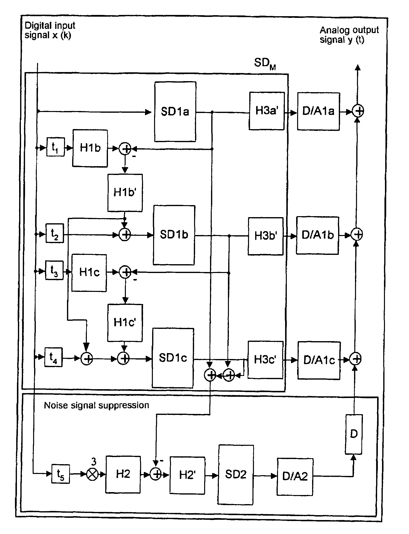
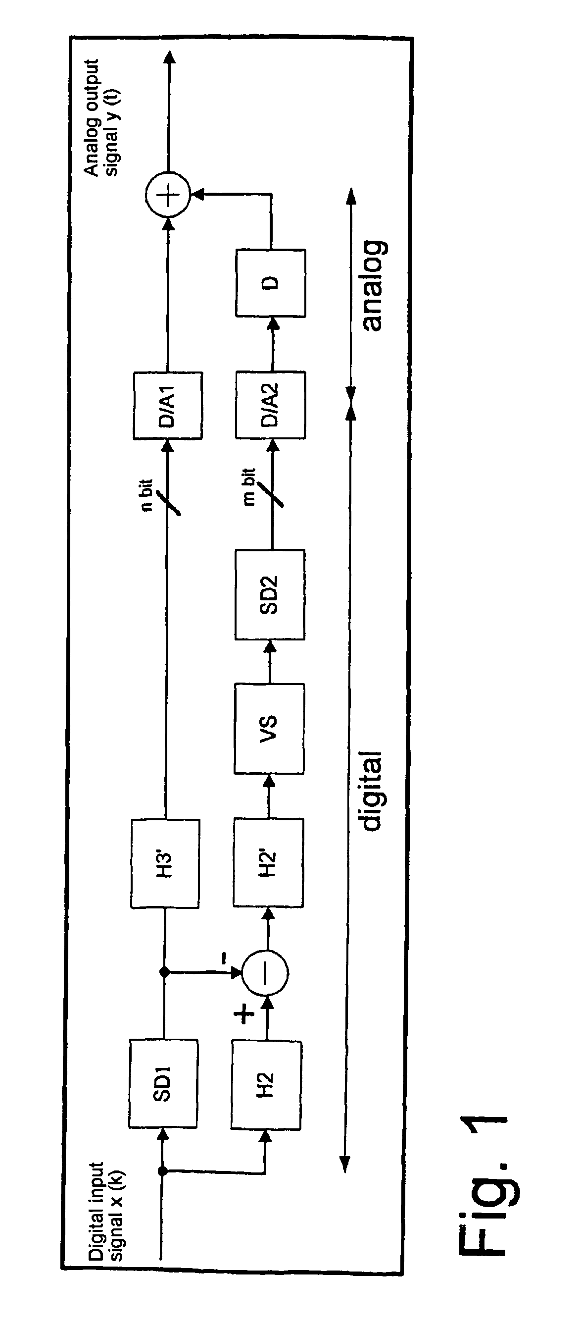
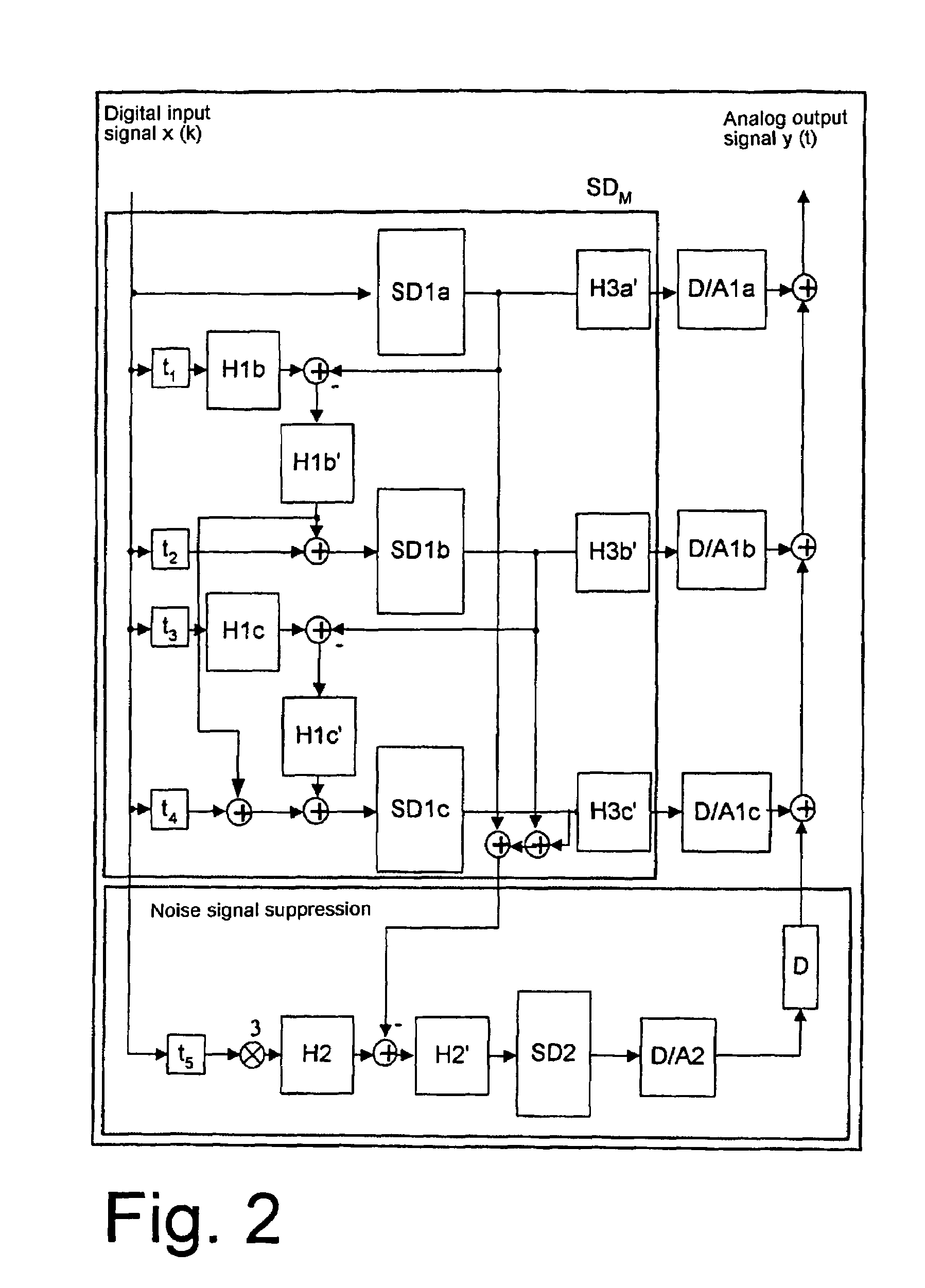
[0038]FIG. 1 shows the basic principle of a sigma-delta converter with noise suppression. A first sigma-delta modulator SD1 in the principal path generates a digital output signal with a bit width restricted to n bits from a digital input signal x(k). Due to this restricted bit width, a quantization error is created which is transformed by the sigma-delta algorithm outside the useful band in accordance with its noise transmission function. Significant noise signal components also fall into the useful band, however, particularly in the case of a low oversampling factor. To suppress these, the digital input signal x(k) is spectrally shaped by a filter H2 in a parallel oath in accordance with the signal transmission function of the first sigma-delta converter SD...


PUM


Abstract

A digital input signal passes through a principal path, containing at least one sigma-delta modulator having a transmission function and a digital-to-analog converter, and at least one parallel path, connected in parallel to the principal path and having at least one sigma-delta modulator and a digital-to-analog converter. The sigma-delta converter produces an analog output signal by summing the analog output signals of the principal and parallel paths. A differential signal from which at least the noise outside a useful band has been filtered is obtained from the digital output signal of the sigma-delta modulator of the principal path and the input signal that has been spectrally formed by a filter, according to the transmission function of the sigma-delta modulator in the principal path. This differential signal is supplied as the input signal to the sigma-delta modulator in the parallel path(s).

Description

[0001]This application is a 371 of PCT / EP02 / 14597CROSS REFERENCE TO RELATED APPLICATIONS[0002]This application is based on and hereby claims priority to European Patent Application No. 01130333.6 filed on Dec. 19, 2001, the contents of which are hereby incorporated by reference.BACKGROUND OF THE INVENTION[0003]1. Field of the Invention[0004]The invention relates to a sigma-delta converter for converting a digital input signal into an analog output signal.[0005]2. Description of the Related Art[0006]In digital to analog converters, as employed in digital radio communication reception devices for example, a digital input signal with 2N signal states and a fixed sampling frequency fa is usually transposed into an analog signal which should match the digital signal as well as possible in the frequency range −fa / 2 to +fa / 2.[0007]In the case of high bit widths N in particular, the quantity of signal states to be implemented by analog circuit technology represents a fundamental problem sin...

Claims


Application Information

Patent Timeline
Patent Type & Authority Patents(United States)
IPC IPC(8): H03M3/00H03M3/04
CPCH03M3/50H03M7/3022
Inventor JELONNEK, BJORN
Owner NOKIA SIEMENS NETWORKS GMBH & CO KG
Why Eureka
Try Eureka