Semiconductor module including semiconductor memory device shiftable to test mode as well as semiconductor memory device used therein

a semiconductor memory and module technology, applied in the field of semiconductor modules, can solve the problems of inability to detect signal svih, inability to shift each of the drams in the module to the test mode,

Inactive Publication Date: 2006-03-21
RENESAS ELECTRONICS CORP
View PDF14 Cites 34 Cited by
  • Summary
  • Abstract
  • Description
  • Claims
  • Application Information

AI Technical Summary

Benefits of technology

[0028]When shifting to the test mode, the semiconductor memory device is shifted to the test mode in accordance with deactivation of the PLL circuit. According to the invention, therefore, the semiconductor memory device in the module can be accurately shifted to the test mode.
[0032]In the test mode, the bypass signal is generated. When the bypass signal is generated, the external input signal formed of the high voltage level is directly applied to the semiconductor memory device. According to the invention, therefore, the semiconductor memory device in the module can accurately shift to the test mode.

Problems solved by technology

Therefore, such a problem occurs that each of the DRAMs in the module cannot be shifted to the test mode for performing the special operation test.
Therefore, it is impossible to detect signal SVIH within one cycle of the clock signal having a frequency of 50 MHz or more, at which RDIMM operates, and each DRAM in the module cannot shift to the test mode.

Method used


Image

  • Semiconductor module including semiconductor memory device shiftable to test mode as well as semiconductor memory device used therein
  • Semiconductor module including semiconductor memory device shiftable to test mode as well as semiconductor memory device used therein
  • Semiconductor module including semiconductor memory device shiftable to test mode as well as semiconductor memory device used therein

Examples


first embodiment

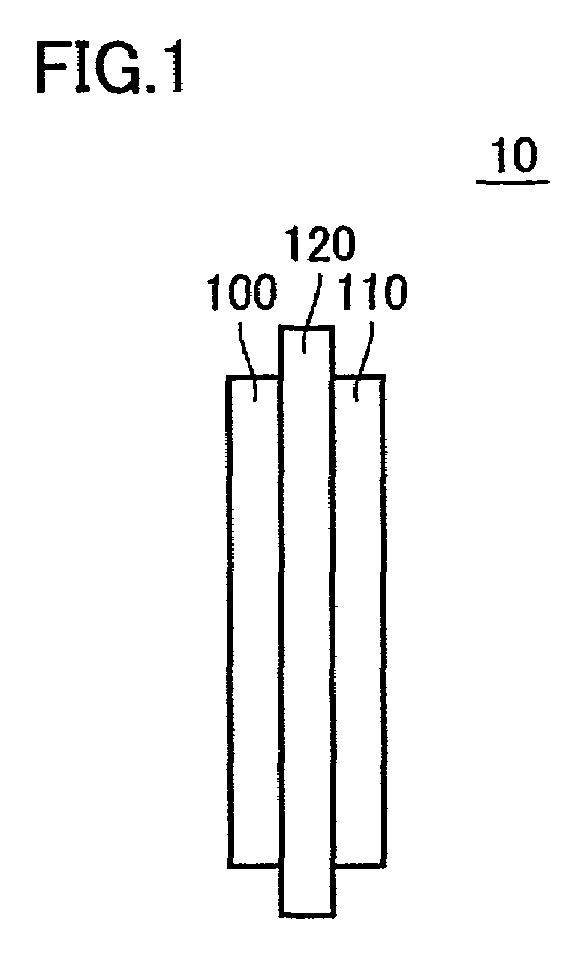
[0083]Referring to FIG. 1, a module 10 includes semiconductor modules 100 and 110, and a substrate 120. Semiconductor modules 100 and 110 are arranged on the opposite sides of substrate 120, respectively. Module 10 is an RDIMM, and semiconductor modules 100 and 110 include a plurality of DRAMs forming the RDIMM.

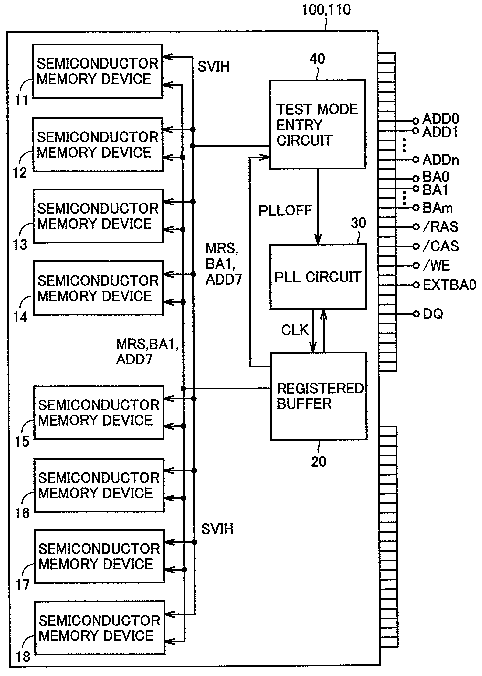
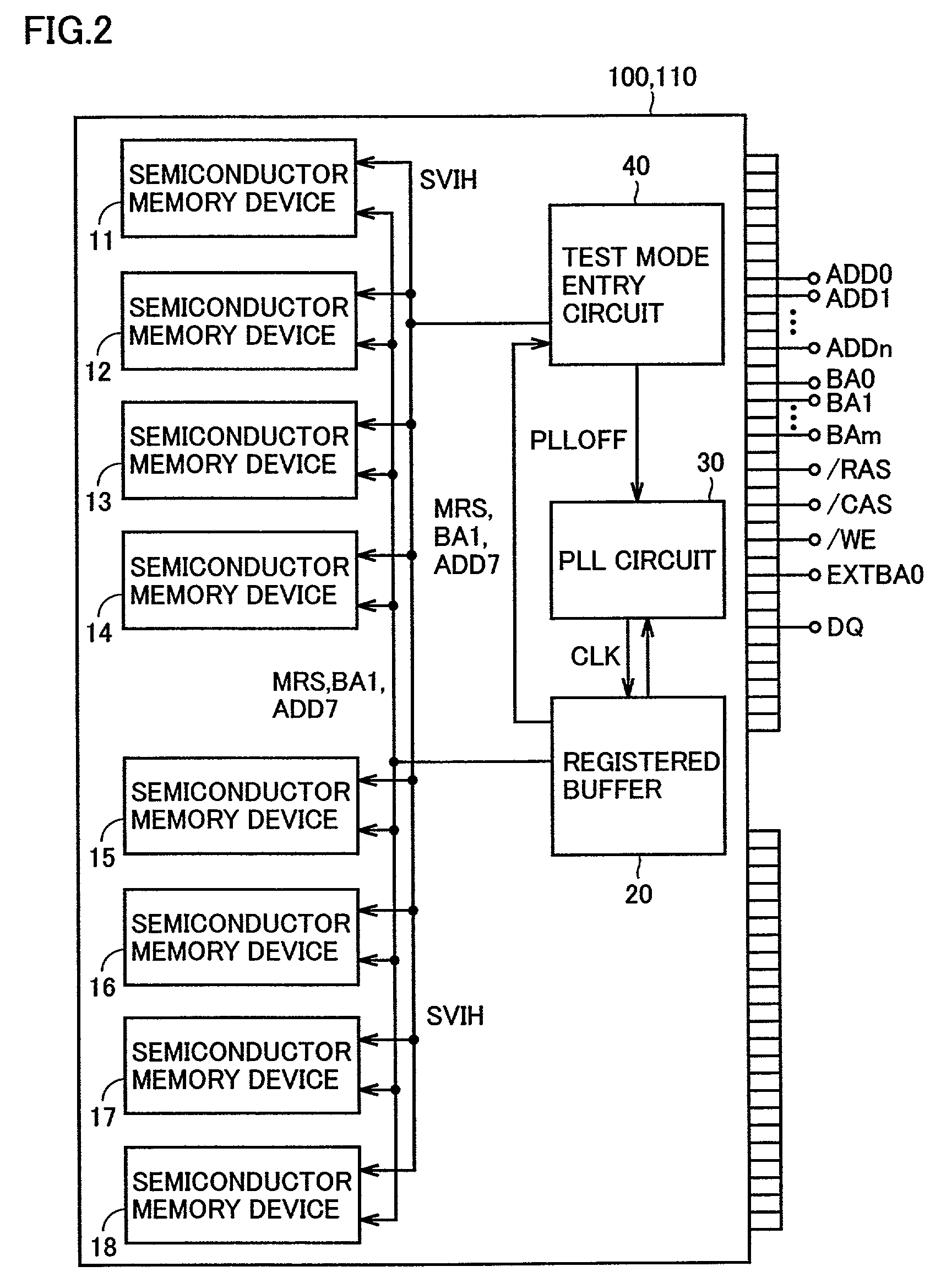
[0084]Referring to FIG. 2, each of semiconductor modules 100 and 110 according to the first embodiment includes semiconductor memory devices 11–18, a registered buffer 20, a PLL circuit 30 and a test mode entry circuit 40.

[0085]Each of semiconductor memory devices 11–18 is formed of a DRAM including a plurality of memory cells, and stores data. Registered buffer 20 receives address signals ADD0–ADDn, bank address signals BA0–BAm, row address strobe signal / RAS, column address strobe signal / CAS, write enable signal / WE and data from external terminals, and converts the received address signals ADD0–ADDn and others to predetermined voltage levels for use in semiconductor modul...

second embodiment

[0134]Referring to FIG. 8, semiconductor modules 100A and 110A of a second embodiment differ from semiconductor modules 100 and 110 of the first embodiment in that a signal generating circuit 40A is employed instead of test mode entry circuit 40. The structures other than the above are the same. However, registered buffer 20 has the same function as that in the first embodiment, and additionally has a function of directly supplying signal EXTBA0, which is formed of the voltage level higher than the voltage level in the normal operating range, to semiconductor memory devices 11–18 without converting signal EXTBA0 to the voltage level for use in the module. Semiconductor modules 100A and 110A are used in module 10 instead of semiconductor modules 100 and 110 shown in FIG. 1, and form the RDIMM.

[0135]Referring to FIG. 9, signal generating circuit 40A is formed of an AND gate 400. AND gate 400 performs the logical AND among signal MRS, bank address signal BA1 and address signal ADD7 sup...

third embodiment

[0150]Referring to FIG. 12, semiconductor modules 100B and 110B according to a third embodiment differ from semiconductor modules 100 and 110 in that test mode entry circuit 40 is not employed, and semiconductor memory devices 11A–18A are employed instead of semiconductor memory devices 11–18. Structures other than the above are the same as those of semiconductor modules 100 and 110. However, semiconductor modules 100B and 110B are not externally supplied with signal EXTBA0 formed of a high voltage level. When shifting to the test mode, registered buffer 20 outputs an address signal ADD9 to semiconductor memory devices 11A–18A in addition to signal MRS, bank address signal BA1 and address signal ADD7. Semiconductor modules 100B and 110B are used in module 10 instead of semiconductor modules 100 and 110 shown in FIG. 1, and form the RDIMM.

[0151]Referring to FIG. 13, semiconductor memory devices 11A–18A differ from semiconductor memory devices 11–18 in that mode circuit 280 is replace...


PUM


Abstract

A semiconductor module includes a plurality of semiconductor memory devices, a registered buffer, a PLL circuit and a test mode entry circuit. The test mode entry circuit receives a signal MRS, a bank address signal and an address signal from the registered buffer, directly and externally receives a signal formed of a high voltage level higher than the voltage level in a normal operating range, generates a deactivating signal for deactivating the PLL circuit and a test mode shift signal formed of the high voltage level, applying the deactivating signal to the PLL circuit, and applying the test mode shift signal to the plurality of semiconductor memory devices. Consequently, the plurality of semiconductor memory devices included in the module can be shifted to the test mode in the modular state.

Description

BACKGROUND OF THE INVENTION[0001]1. Field of the Invention[0002]The present invention relates to a semiconductor module including a plurality of semiconductor memory devices, and particularly relates to a semiconductor module, which allows the semiconductor memory devices in the module to shift to a test mode for testing a special operation, as well as the semiconductor memory devices used therein.[0003]2. Description of the Background Art[0004]In recent years, attention has been given to a DIMM (Double Inline Memory Module), which operates in synchronization with a clock signal having a frequency of 50 MHz or more. The DIMM has two semiconductor modules formed on the opposite sides of one substrate, respectively. The semiconductor module includes a plurality of DRAMs (Dynamic Random Access Memories).[0005]In particular, the semiconductor module used in a registered DIMM (RDIMM) includes a plurality of DRAMs, a PLL circuit and a registered buffer circuit. The PLL circuit generates a...

Claims


Application Information

Patent Timeline
Patent Type & Authority Patents(United States)
IPC IPC(8): G11C29/00G01R31/28G01R31/3185G06F12/16G11C7/22G11C11/401G11C11/4076G11C29/14G11C29/46
CPCG11C7/22G11C7/222G11C29/46G11C11/4076G11C11/401
Inventor ENDOU, SHUNSUKEMIYAMOTO, TAKAYUKINAKAI, JUN
Owner RENESAS ELECTRONICS CORP
Why Eureka
Try Eureka