Optical information recording and reproducing apparatus and optical information recording apparatus

Inactive Publication Date: 2007-06-28
CANON KK
View PDF5 Cites 9 Cited by
  • Summary
  • Abstract
  • Description
  • Claims
  • Application Information

AI Technical Summary

Benefits of technology

[0009] Hence, an object of the present invention is to provide an optical information recording and reproducing apparatus capable of correcting a shift or compensating the shift even when the shift occurs in the positional relation ship between the light beam incident on the spatial light modulator and the spatial light modulator.
[0012] In the present invention, correcting means, for example, corrects the detected positional shift amount by feedback. Further, as the spatial light modulator, it is preferable to use a modulator having a plurality of pixels and a configuration capable of allowing the effective pixel to function as a pixel for reference beam and a pixel for information beam. When such a spatial light modulator is used, the area of the effective pixel of the spatial light modulator is divided into the area for reference beam and the area for information beam according to the position based on the detected positional shift amount, so that the correction of the positional shift can be performed.
[0018] In the optical information recording and reproducing apparatus of the present invention, in order to detect a shift amount of the light beam, the element configured by semiconductor chips is increased by one just by the shift amount detector typically configured as an image sensor. However, it is possible also to use the light sensing device for hologram reproduction as a shift amount detector, and in that case, as compared to the conventional element, the number of semiconductor chips does not increase. Particularly, by integrally providing the spatial light modulator and the light sensing device on the same substrate, the number of such semiconductor chips can be reduced to one piece from two pieces. Since the spatial light modulator and the light sensing device such as a CMOS sensor are almost the same in each step of the semiconductor process for manufacturing these elements, the increase in the number of steps is not accompanied, and it is possible to incorporate the functions of these elements all at once. As a result, despite the fact that the functions of correcting the positional shift of the light beam is added, the optical system is made much simpler as the optical information recording and reproducing apparatus, thereby making it possible to make a setting space much smaller. Further, since the write to the recording medium and read from the recording medium can be performed approximately on the same axis, the positional shift between the optical system for write and the optical system for read is substantially eliminated, so that the adjustment of the optical shift between both systems are not required.

Problems solved by technology

Further, in the optical information recording and reproducing apparatus of this type, while it is assumed that the laser light source is exchanged, even due to insufficient reproducibility of the physical position at the time of such an exchange of the light source, a shift may occur in the positional relationship between the spatial light modulator and the light beam.
When such a shift occurs, an adequate beam quantity necessary to form the interference fringes is not secured and a part of the interference fringes originally to be formed is lost in the event that the interference fringes (volume hologram) is formed in the recording medium by the reference beam and the information beam.
As a result, an erroneous hologram pattern is recorded in the recording medium, and when the information is reproduced from the recording medium, an erroneous reproduced light is detected.
An erroneous detection of the reproduced light directly leads to the generation of a reproducing error.

Method used


Image

  • Optical information recording and reproducing apparatus and optical information recording apparatus
  • Optical information recording and reproducing apparatus and optical information recording apparatus
  • Optical information recording and reproducing apparatus and optical information recording apparatus

Examples


first embodiment

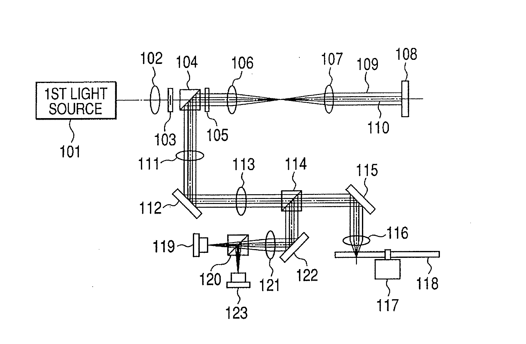
[0060] First, a concept of the correction of a positional shift in the present invention will be described. In a holographic memory system, due to various factors, the positional shift may be generated in the positional relationship between the light beam incident on a two-dimensional spatial light modulator (SLM) and a spatial light modulator. The present invention corrects this shift or attempts at its compensation. The correction of the positional shift will be described below by using FIGS. 1 to 3.

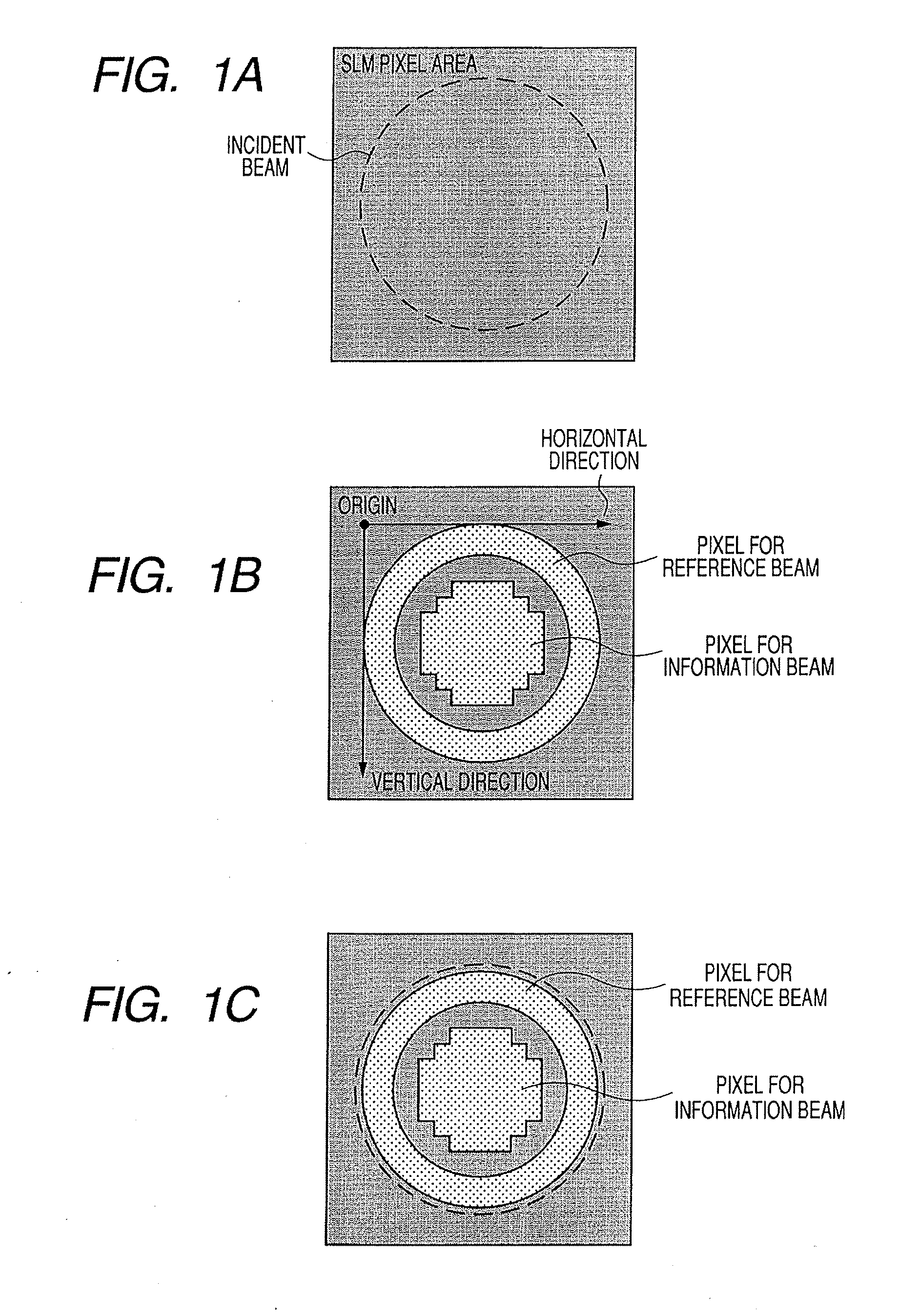
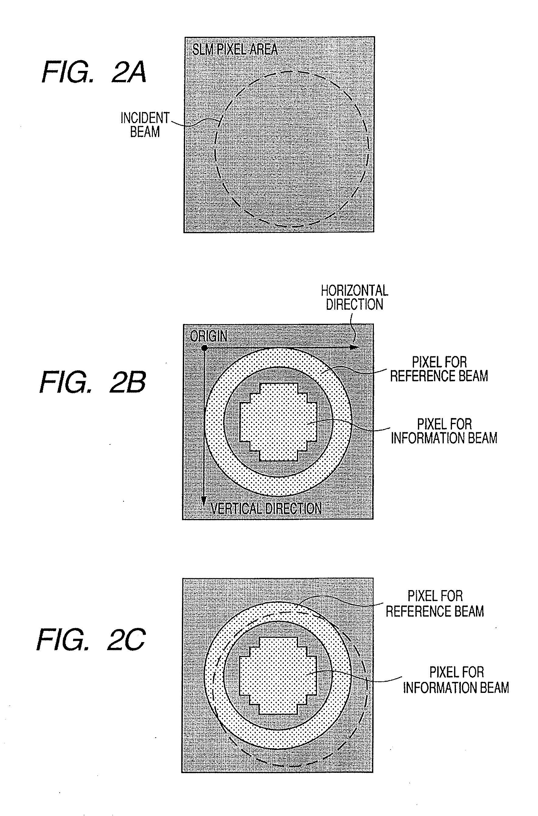
[0061]FIGS. 1A to 1C show a case where the positional relationship between an incident beam on a SLM and the SLM is according to a design. As shown in FIG. 1A, a two-dimensional SLM comprises a square effective pixel area, and inside this effective pixel area, there is arranged a large number of pixels in a matrix pattern. The incident beam is circular, and its diameter is smaller than the effective pixel area of the SLM. If the positional relationship is according to the design, the ...

second embodiment

[0129] In the present invention, as a correction method of the shift of an incident beam to a spatial light modulator, as described above, there is a method of physically moving the spatial light modulator itself according to the shift amount in addition to the method of changing a start position of the shift register and electrically correcting a display position at the spatial light modulator. FIG. 20 is a view explaining about a shift correction by physical movement.

[0130] In FIG. 20, in the surface of the spatial light modulator, an actual incident beam 303 is shifted from a designed incident beam 301. Directly below the spatial light modulator, a light sensing device area of a CMOS sensor is provided, and each light receiving pixel shall be shown by reference numeral 302. Further, a point that serves as a reference for the operations of a horizontal shift register and a vertical shift register is an origin 310. In the present embodiment, for such a shift, as shown in FIG. 20, ...

third embodiment

[0131] In the above described first embodiment, while the modulator / light sensing device 108 has been configured by laminating the spatial light modulator (SLM) and the light sensing device (CMOS sensor) on the surface of the silicon semiconductor substrate in a vertical direction, the modulator / light sensing device used in the present invention is not limited to this. In the modulator / light sensing device 108, the spatial light modulator and the light sensing device may be arranged in a horizontal posture for each pixel. FIG. 21 shows the modulator / light sensing device 108 in which the SLM and the light sensing device are arranged in such a horizontal posture.

[0132] The modulator / light sensing device 108 shown in FIG. 8 comprises a SLM element area 64 having the SLM composed of a reflection type light interference modulator and a CMOS sensor area 65 having a CMOS light sensing device for each pixel. The SLM element area 64 and the CMOS sensor area 65 for each pixel are provided in...


PUM


Abstract

An object is to be able to correct a shift even when the shift occurs in the light beam incident on a spatial light modulator in an optical information recording apparatus such as a hologram memory system and the like using the spatial light modulator having an area to modulate information beam. Hence, a shift amount detector is provided, which detects a shift of the light beam incident from a first light source on the spatial light modulator (modulator / light sensing device). Based on the shift amount detected by the shift amount detector, a position of the information beam modulating area in the spatial light modulator is shifted from an initial position.

Description

BACKGROUND OF THE INVENTION [0001] 1. Field of the Invention [0002] The present invention relates to an optical information recording and reproducing apparatus and an optical information recording apparatus using a hologram capable of recording information with a higher density and a larger capacity by recording optical interference fringes on a recording medium. [0003] 2. Description of the Related Art [0004] These days, the world has entered an age of multimedia, and the necessity for a recording apparatus that performs a recording for a recording medium and a recording and reproducing apparatus that performs recording and reproducing for a recording medium has increased a level of importance, and its recording density has been raised year by year. In an optical information recording medium also, a progress has been made from a CD (compact disk) through a DVD (Digital versatile disk) to a BlueRay (Blue ray) disk. Responding to the progress made in the optical information recording...

Claims


Application Information

Patent Timeline
IPC IPC(8): G11B7/00
CPCG11B7/0065G11B7/083G11B7/128
Inventor SAKAGUCHI, KIYOFUMIICHIKAWA, TAKESHI
Owner CANON KK
Why Eureka
Try Eureka