Photomask defect correction method employing a combined device of a focused electron beam device and an atomic force microscope

a technology of atomic force microscope and electron beam, which is applied in the field of photomask defect correction method employing a combined device of focused electron beam device and atomic force microscope, can solve the problems of not knowing the position and shape of defects, difficult to search for defects, and finding the position of defects is more time-consuming than processing, so as to shorten the time of taking out and insertion of the mask. , the effect of shortening the tim

Active Publication Date: 2008-05-20
HITACHI HIGH TECH SCI CORP
View PDF5 Cites 9 Cited by
  • Summary
  • Abstract
  • Description
  • Claims
  • Application Information

AI Technical Summary

Benefits of technology

[0011]In order to resolve the aforementioned problems, a device is employed that combines an electron beam device having the features of high resolution, short observation time, little damage imparted on a sample when observing an image and clear defect correction capabilities and an AFM scratch processor having the feature of being capable of precise dark defect correction. The following methods are then carried out using this device.
[0014]With clear defect correction, first, a clear defect is irradiated with a focused electron beam while providing light-blocking layer source gas so that a light-blocking film is deposited on a clear defect region protruding from a normal pattern. After that, the protruding portion is removed by AFM scratch processing as with the opaque defect correction. It is therefore possible to correct small clear defects with a high degree of precision in this manner.
[0016]By observing using a focused electron beam it is therefore possible to reduce the number of times of image observation using AFM where position alignment taking five to ten minutes each time after changing a tip takes place. This means that time-consuming changing of the tip and subsequent alignment of the tip can be made to happen more quickly. A device is used where an electron beam and an AFM are combined within a vacuum. Evacuating the vacuum and releasing the air take in the order of ten minutes. However, high-magnification observations depend on time-consuming AFM observations. It is therefore possible to make the total correction time short compared with conventional systems of the related art composed of an AFM and an optical microscope.
[0017]It is possible to omit time-consuming AFM imaging by carrying out determinations in a direction (rotational direction of the stage) necessary for a vertical cross-section. This means it is possible for the total correction time to be made short even if the vacuum exhaust time and the atmosphere discharge time are time-consuming.
[0018]It is also possible to omit the AFM imaging that took time in the related art because the calculation of a shift compensation amount for an angle of fitting to the vertical surface of the processing tip is carried out using a secondary electron image of a focused electron beam. It is therefore possible to make the total time short. The extent of shift of an angle of fitting to the vertical surface of the processing tip is corrected using rotation of the stage. The XY stage is then moved so as to correct shifts in the XY position. Extraction of the defect position is then carried out using the secondary electron image of the focused electron beam. It is therefore possible to omit the time-consuming AFM imaging of the related art and total time can be made shorter.
[0020]By using a device where the focused electron beam and the AFM scratch unit are in a vacuum, it is possible to shorten the time of taking out and inserting the mask and performing mask alignment, and correct an overcut location using opaque defect correction for AFM scratch processing in a shorter period of time compared with the case of other devices of the related art.

Problems solved by technology

It is therefore not possible to know the positions and shapes of defects even when an optical microscope is at maximum magnification because the defects are too small.
Image acquisition therefore has to be carried out using an AFM image, which is time-consuming.
It is also difficult to search for defects with a field of vision of 40 μm even with an AFM image.
Finding the positions of the defects is therefore more time-consuming than the processing.
Because of this, it is therefore necessary to carry out mask alignment so as to re-link the defect scanning device and defect coordinates so as to obtain an image and then perform a time-consuming search for defects using an AFM image, which is still more time-consuming.
In addition to opaque defects that are surplus to a pattern in a photomask, there also exist clear defects that are pattern deficiencies, and in theory, it is not possible for the AFM scratch processing device to correct clear defects.
However, various problems occur such as thin films of 0.1 μm or less not becoming attached, sagging occurring in the shapes of the films so that transmittance is lowered by a hollow component, and charging up occurring in order to correct a photomask constituted by an insulator so as to cause positional precision to fall.
In addition to this, at the time of correction using an AFM scratch processing device, in the event that opaque defects are overcut, it is not possible to achieve anything by just using an AFM scratch processing device that can only perform elimination processing.
In this case, correction of overcut portions takes place using a clear defect correction function of an FIB or electron beam device but high-precision correction of defects of a level small enough to enable correction using an AFM scratch processor was not possible.
In cases where it is necessary to alternately use AFM scratch processing devices and FIB and electron beam devices a plurality of times, the number of times it is necessary to output positions of defects using time-consuming AFM scratch processing increases, which causes operation time to increase substantially.
Further, at the time of use of the FIB and electron beam device, time is required every time vacuuming takes place and to await the release of the atmosphere, re-alignment of the mask is necessary every time a mask is replaced, which is an extremely time-consuming operation.

Method used


Image

  • Photomask defect correction method employing a combined device of a focused electron beam device and an atomic force microscope
  • Photomask defect correction method employing a combined device of a focused electron beam device and an atomic force microscope
  • Photomask defect correction method employing a combined device of a focused electron beam device and an atomic force microscope

Examples


Embodiment Construction

[0025]The following is a description of an embodiment of the present invention.

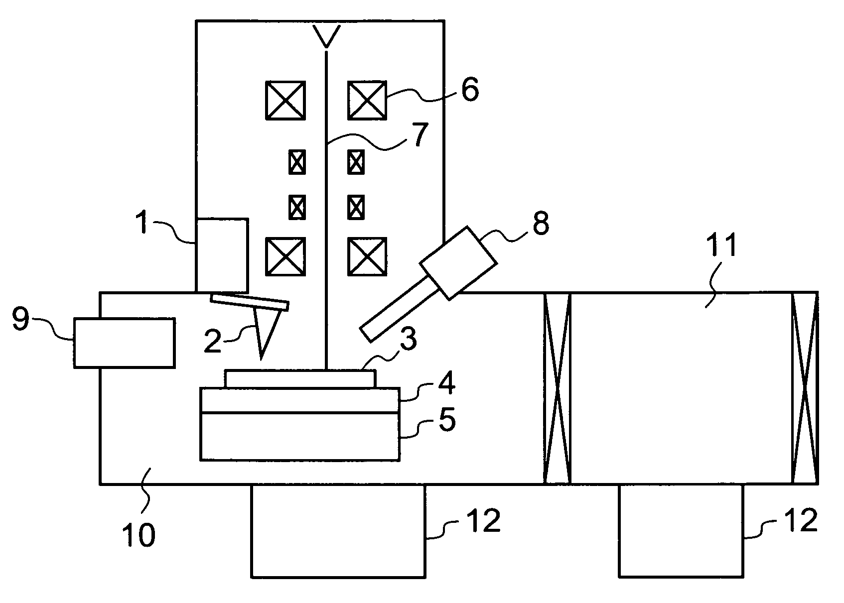
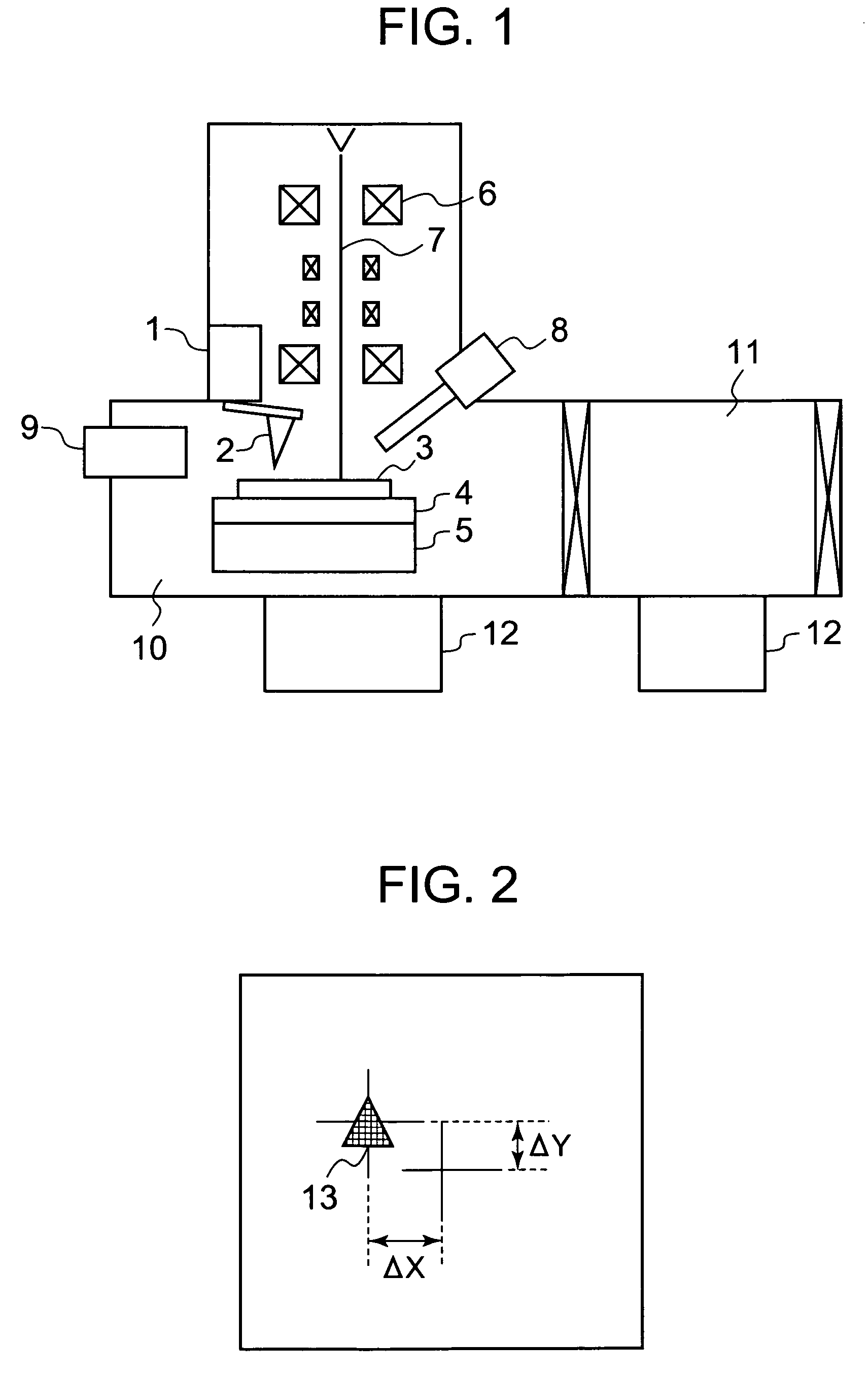
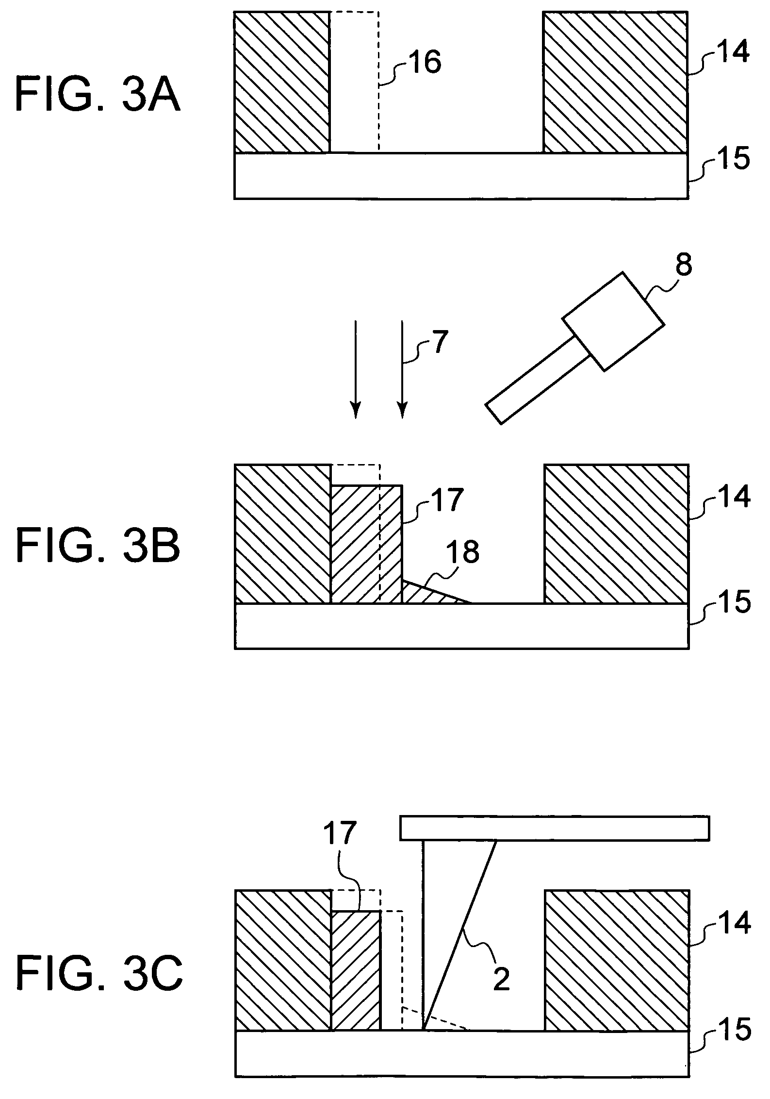
[0026]FIG. 1 shows a combined device of a focused electron beam device and AFM used in the present invention. A photomask 3 for which a defect has been found using a defect scanning device is introduced into a preliminary chamber or pre-chamber 11 of a device combining an electro-optical system 6 and an atomic force microscope (AFM) head 1 within a container having a vacuum evacuation system 12, and preliminary evacuation is carried out. When a vacuum is created in the preliminary chamber 11, the photomask 3 is moved into a work chamber 10 and placed on a rotating stage 4 supported on an XY stage 5. In the combined device, the work chamber 10 is common to and shared by the focused electron beam device and the AFM. An alignment mark of the mask is then observed at a high-magnification by detecting secondary electrons generated from the sample owing to irradiation of the focused electron beam 7 with the sec...


PUM

PropertyMeasurementUnit
atomic force microscopeaaaaaaaaaa
defect sizeaaaaaaaaaa
angleaaaaaaaaaa

Abstract

In order to make it possible to improve throughput of AFM scratch processing, enable correction of small defects in clear defect correction with a high degree of precision, and enable correction in a shorter period of time in the event of overcutting by AFM scratch processing, throughput of AFM scratch processing is increased by maximizing high-resolution of the electron beam device and minimizing the time taken in observations using a device incorporating both an electro-optical system and an AFM head in a vacuum, correcting small clear defects with high precision by eliminating portions left over from AFM scratch processing after applying a clear defect correction film using an electron beam while providing light-blocking film raw material, and correction in a short time is made possible by eliminating portions remaining using AFM scratch processing after applying a clear defect correction film using an electron beam while providing light-blocking film raw material also in cases of overcutting in AFM scratch processing.

Description

BACKGROUND OF THE INVENTION[0001]1. Field of the Invention[0002]The present invention relates to a photomask defect correction method employing a combined device of a focused electron beam device and an atomic force microscope.[0003]2. Description of the Related Art[0004]As fine detailing of patterns becomes smaller, photomask defects of an original plate of a pattern transfer for a wafer to be corrected also become small, and high-precision correction can also be obtained. Further, optical proximity correction (OPC) patterns that are even smaller patterns for correcting optical proximity results so as to increase resolving power have also been introduced which means that it is also necessary to correct defects of OPC patterns that are smaller than these patterns. In addition to defect correction devices employing lasers and focused electron beams of the related art, it is also possible to carry out scratch processing of physically eliminating opaque defects using a diamond tip that...

Claims


Application Information

Patent Timeline
Patent Type & Authority Patents(United States)
IPC IPC(8): G01N23/04G01N13/16G01N23/00G03F1/72G21K7/00H01L21/027
CPCG01N23/00G03F1/72G03F1/74B82Y35/00G01Q30/02G01Q60/24G01Q80/00Y10S977/856
Inventor TAKAOKA, OSAMUHAGIWARA, RYOJI
Owner HITACHI HIGH TECH SCI CORP
Why Eureka
Try Eureka