Wire bonding method and wire bonding apparatus

a wire bonding and wire bonding technology, applied in the direction of soldering apparatus, manufacturing tools,auxillary welding devices, etc., can solve the problems of insufficient bonding and bonding failure of wires, and achieve the effect of eliminating bonding failures and eliminating bonding failures

Inactive Publication Date: 2006-03-28
SEIKO EPSON CORP
View PDF5 Cites 32 Cited by
  • Summary
  • Abstract
  • Description
  • Claims
  • Application Information

AI Technical Summary

Benefits of technology

[0009]In accordance with the present invention, the tip portion of the wire is bonded to the first electrode by the first tool, and a portion of a section of the wire that is lead out from the first electrode is bonded to the second electrode by the second tool. The width of the open end section of the second hole is made greater than the width of the open end section of the first hole. Accordingly, the pressing area of the wire can be sufficiently secured, and the wire can be securely bonded to the second electrode, such that bonding failures can be eliminated.
[0021]A wire bonding apparatus in accordance with the present invention comprises first and second tools for bonding a wire to first and second electrodes, wherein the first tool includes a first hole through which the wire is passed and an open end section of the first hole that is pressed against a tip portion of the wire that protrudes outside the first hole, the second tool includes a second hole through which the first tool is passed and an open end section of the second hole, and the open end section of the first hole and the open end section of the second hole are pressed against a part of a section of the wire that is lead out from the first electrode. In accordance with the present invention, the open end section of the first hole and the open end section of the second hole are pressed against a portion of a section of the wire that is lead out from the first electrode. Accordingly, the pressing area of the wire can be sufficiently secured, and the wire can be securely bonded to the second electrode, such that bonding failures can be eliminated.

Problems solved by technology

However, as the reduction of the diameter of the tip portion of each capillary advances, the tip portions of the capillaries and the wires have reduced contact areas when the wires are bonded to the leads (in second bonding), such that the wires may not be sufficiently bonded to the leads, which occasionally caused bonding failures.

Method used


Image

  • Wire bonding method and wire bonding apparatus
  • Wire bonding method and wire bonding apparatus
  • Wire bonding method and wire bonding apparatus

Examples


Embodiment Construction

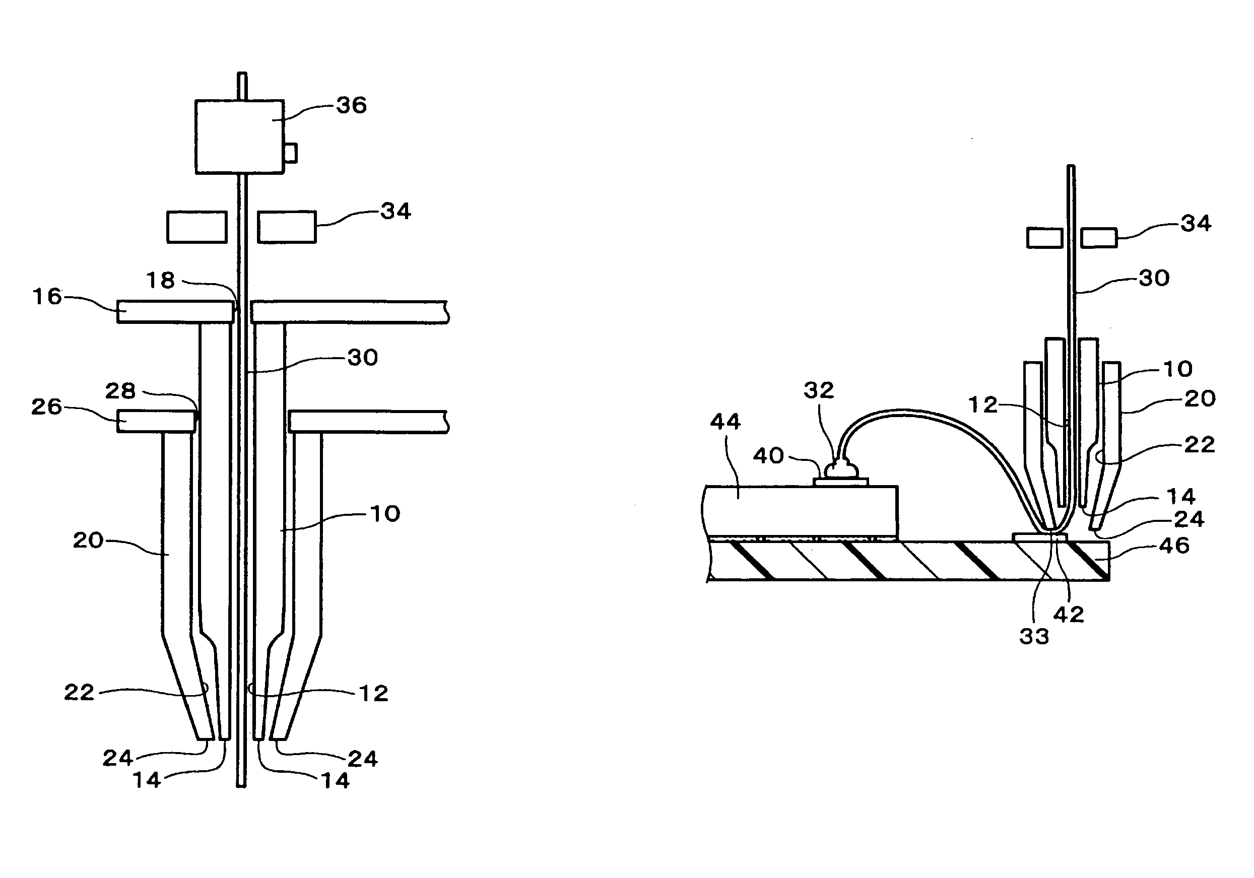
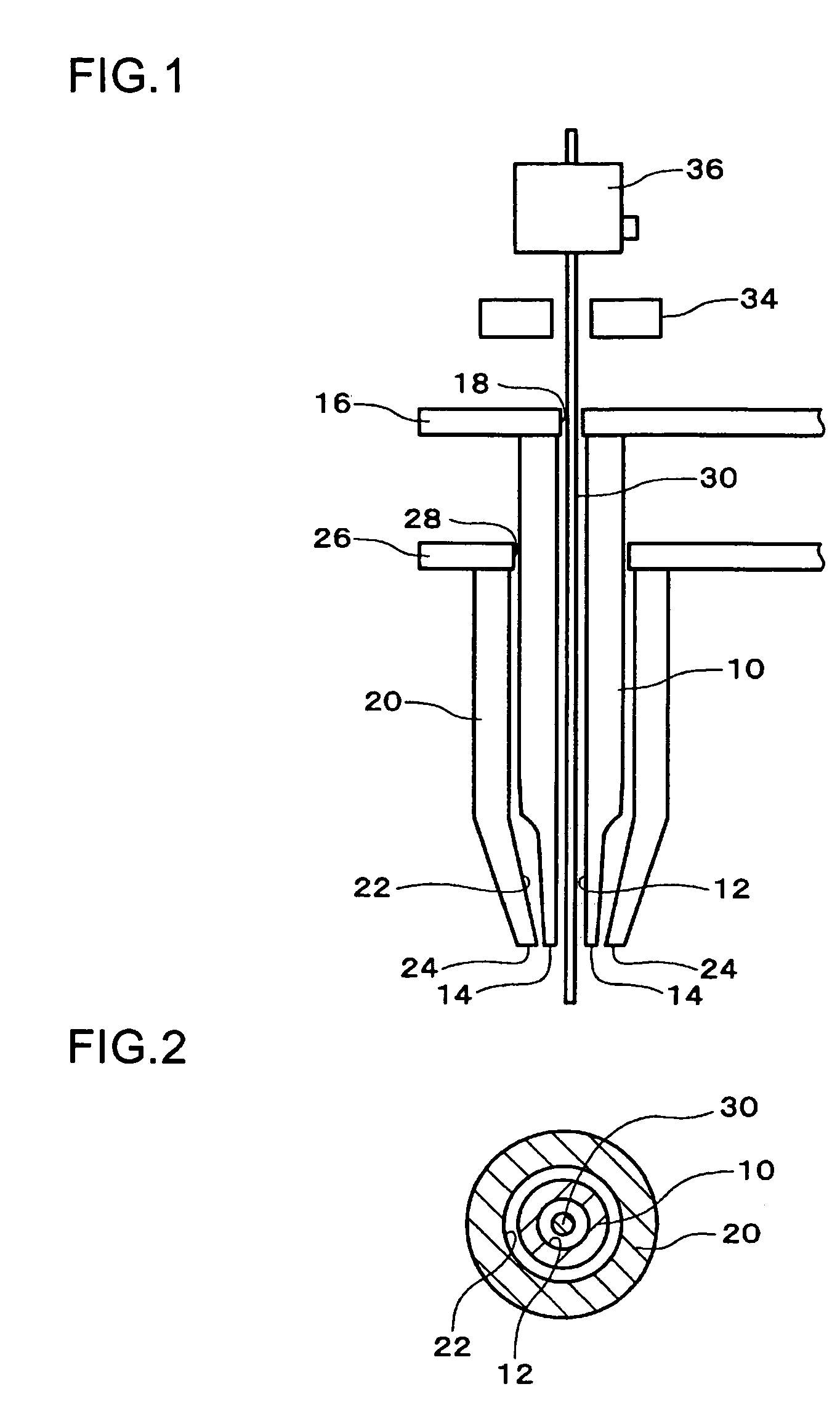
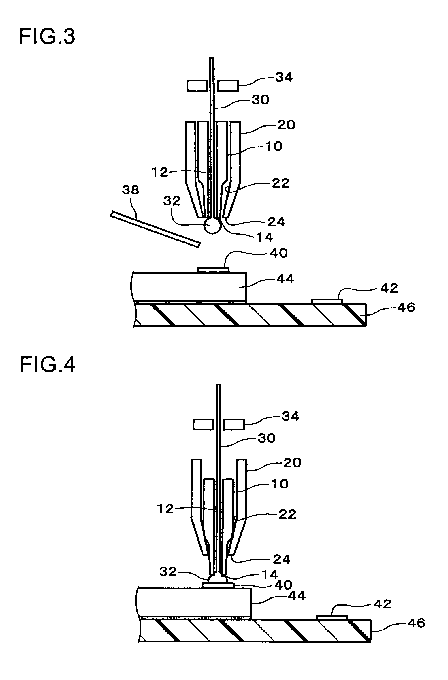
[0032]Hereafter, an embodiment of the present invention will be described with reference to the drawings. FIG. 1 and FIG. 2 are diagrams for describing a wire bonding apparatus in accordance with an embodiment of the present invention. When manufacturing a semiconductor device, the wire bonding apparatus functions as an apparatus that manufactures the semiconductor device. The wire bonding apparatus is used for conducting a ball bonding (or nail head bonding) process.

[0033]The wire bonding apparatus includes first and second tools (for example, first and second capillaries) 10 and 20. For example, the wire bonding apparatus includes a work piece (for example, a semiconductor device) supply section, a transfer section and storage section, a bonding head section, and a table on which the bonding head section is mounted. The first and second tools 10 and 20 are attached to holders (supporting members 16 and 26) of the bonding head section, and can be moved in three dimensions by operat...


PUM

PropertyMeasurementUnit
widthaaaaaaaaaa
areaaaaaaaaaaa
heightaaaaaaaaaa

Abstract

A highly reliable bonding process is provided. The wire bonding method includes: (a) bonding a tip portion of a wire to a first electrode by pressing an open end section of a first hole of a first tool against the tip portion of the wire that is passed through the first hole and protrudes outside the first hole, and (b) bonding a part of a section of the wire that is lead out from the first electrode to a second electrode. The first tool is passed through a second hole of a second tool. The width of an open end section of the second hole is formed greater than the width of the open end section of the first hole. The step (b) is conducted by pressing the open end section of the second hole against the part of the wire.

Description

CROSS-REFERENCE TO RELATED APPLICATIONS[0001]The present application claims priority to Japanese Patent Application No. 2003-005966 filed Jan. 14, 2003 which is incorporated by reference in its entirety.BACKGROUND OF THE INVENTION[0002]1. Technical Field[0003]The present invention relates to a wire bonding method and a wire bonding apparatus.[0004]2. Related Art[0005]In a wire bonding process that is conducted in the manufacturing of semiconductor devices, pads of a semiconductor chip and leads of a package are connected with wires. In this process, tip portions of the wires that are lead outside from ends of capillaries are bonded to pads, the wires are lead out from the pads, and parts thereof are bonded to the leads. Recently, due to further miniaturization and higher integration of semiconductor devices, pads of semiconductor chips have become finer and the pitch thereof has become narrower. In an attempt to prevent the wires from contacting one another, the tip portion of each ...

Claims


Application Information

Patent Timeline
Patent Type & Authority Patents(United States)
IPC IPC(8): B23K31/02B23K20/00H01L21/60B23K20/10H01L21/603H01L21/607
CPCH01L24/32B23K20/005B23K20/007B23K20/106H01L24/78H01L24/83H01L24/85H01L2924/14H01L2924/15311H01L2924/01082H01L2924/01033H01L2924/01013H01L2924/01006H01L2924/01005H01L2924/01004H01L2224/92247H01L2224/85181H01L2224/85045H01L2224/83801H01L2224/8319H01L2224/78302H01L2224/78268H01L2224/73265H01L2224/48465H01L2224/48247H01L2224/48227H01L2224/32225H01L2224/32245H01L2224/48091H01L2924/00014H01L2924/00H01L2924/00012H01L2224/85205H01L2924/00011H01L2224/85203H01L2924/181H01L24/73H01L24/48H01L2224/78301H01L2224/45099H01L2224/83205
Inventor NOSAKA, HITOSHI
Owner SEIKO EPSON CORP
Why Eureka
Try Eureka