Light-emitting diode light source unit

a light source unit and diode technology, applied in the association of printed circuit non-printed electric components, lighting support devices, printers, etc., can solve the problem that the irregularity of the illumination intensity of the entire led array due to the irregularity of the reflecting face may effectively be restricted, and achieve good reflection properties, easy formation, and high surface precision

Inactive Publication Date: 2006-03-28
NORITSU PRECISION CO LTD
View PDF5 Cites 7 Cited by
  • Summary
  • Abstract
  • Description
  • Claims
  • Application Information

AI Technical Summary

Benefits of technology

[0008]With this construction, by the groove forming technique, a groove is formed in the printed circuit board constituting the light-emitting diode light source unit. And, a bottom face of this groove serves as a mounting face for mounting the LED elements and a lateral face of the groove serves as a reflecting face disposed laterally of the mounted LED elements for reflecting the beam from the LED elements toward an object to the illuminated. Hence, by implementing an appropriate groove forming technique favorable for obtaining high surface precision, a reflecting face having good reflecting property can be formed with precision along the array of the plurality of LED elements disposed linearly. As a result, the illumination intensity irregularity of the entire LED array due to the irregularity in the reflecting face may be effectively restricted. Further, with the above construction, the reflecting face can be easily formed by only forming the groove in an area of the printed circuit board where the array of LED elements is to be mounted. Thus, this construction eliminates any special separate reflector, thereby to allow the entire construction compact.
[0009]As described above, the lateral face of the groove within which the LED elements are mounted serves as the reflecting face for the LED elements. Therefore, the present invention proposes some particularly advantageous groove shapes all providing a superior reflecting property to that of a simple groove having a rectangular cross section. One example thereof is to form the lateral face of the groove as an inclined face flared open upward from the bottom face of the groove. With this construction, the beam emitted laterally of the LED element will be changed in direction toward a front optical axis of the LED element (where a condensing lens will generally be disposed). According to a further preferred groove shape, the lateral face of the groove is formed as a concave curved face flared open from the bottom face. By providing such reflecting curved face laterally of the LED element, the beam emitted from the LED element can be well focused.
[0010]It is difficult or costly to form a wiring land (wiring pattern) in the bottom face of the groove formed in the printed circuit board. Hence, it is preferred that the bottom face of the groove be used only as the mounting face for mounting the LED elements. In view of this, according to one preferred embodiment of the present invention, a wiring land for the LED elements formed on the surface of the printed circuit board and the LED elements are connected to each other via bonding wires. The use of this wire bonding technique advantageously eliminates the necessity of forming the printed circuit wiring in the bottom face of the groove.

Problems solved by technology

As a result, the illumination intensity irregularity of the entire LED array due to the irregularity in the reflecting face may be effectively restricted.

Method used


Image

  • Light-emitting diode light source unit
  • Light-emitting diode light source unit
  • Light-emitting diode light source unit

Examples


Embodiment Construction

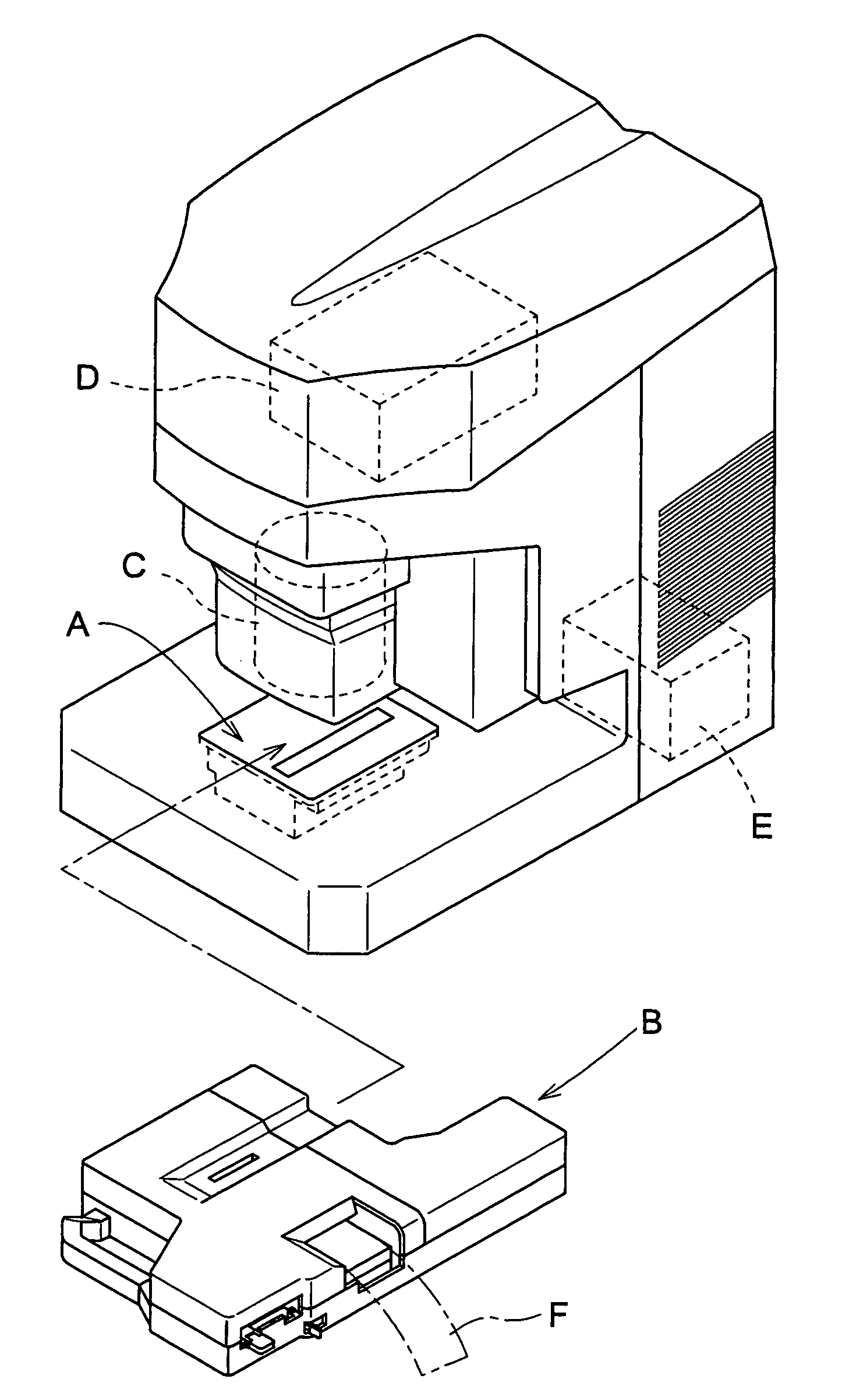
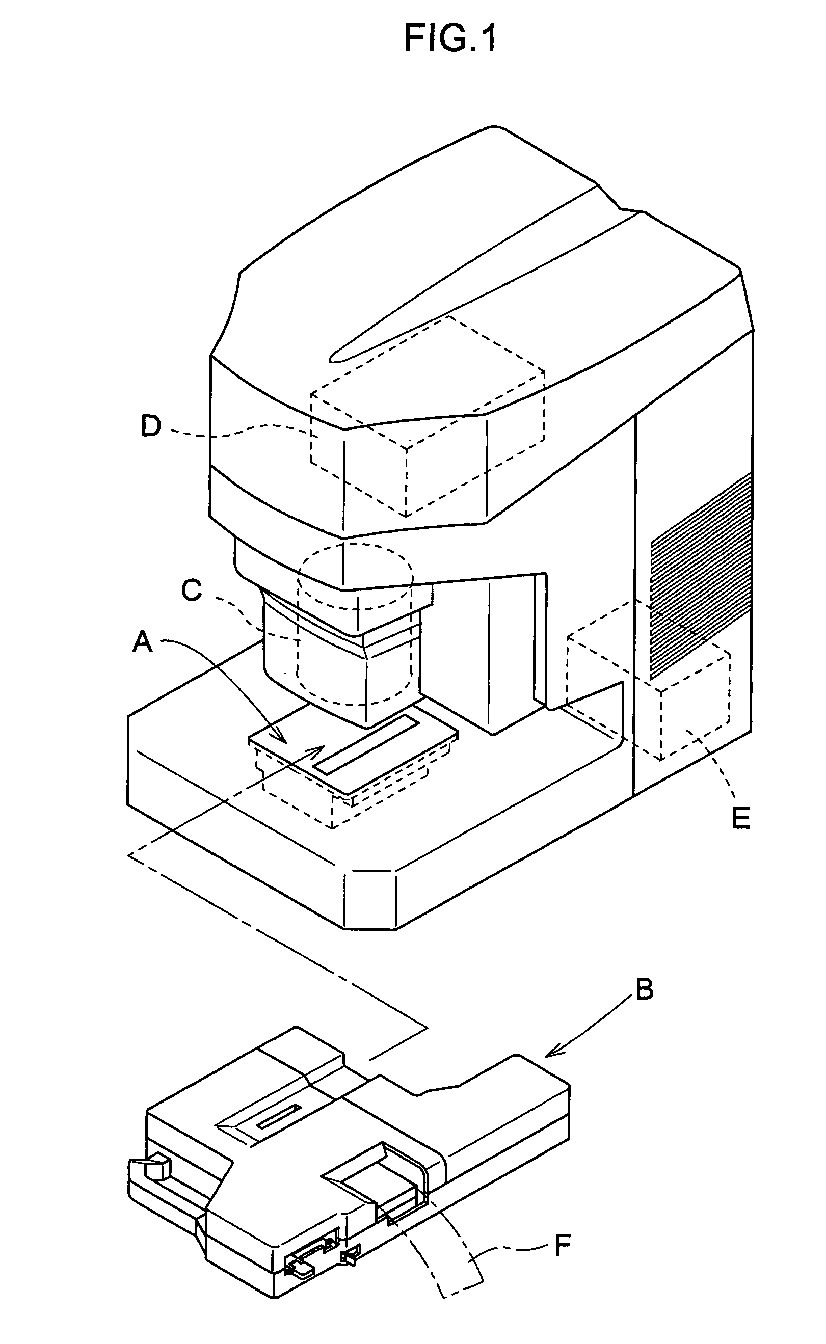
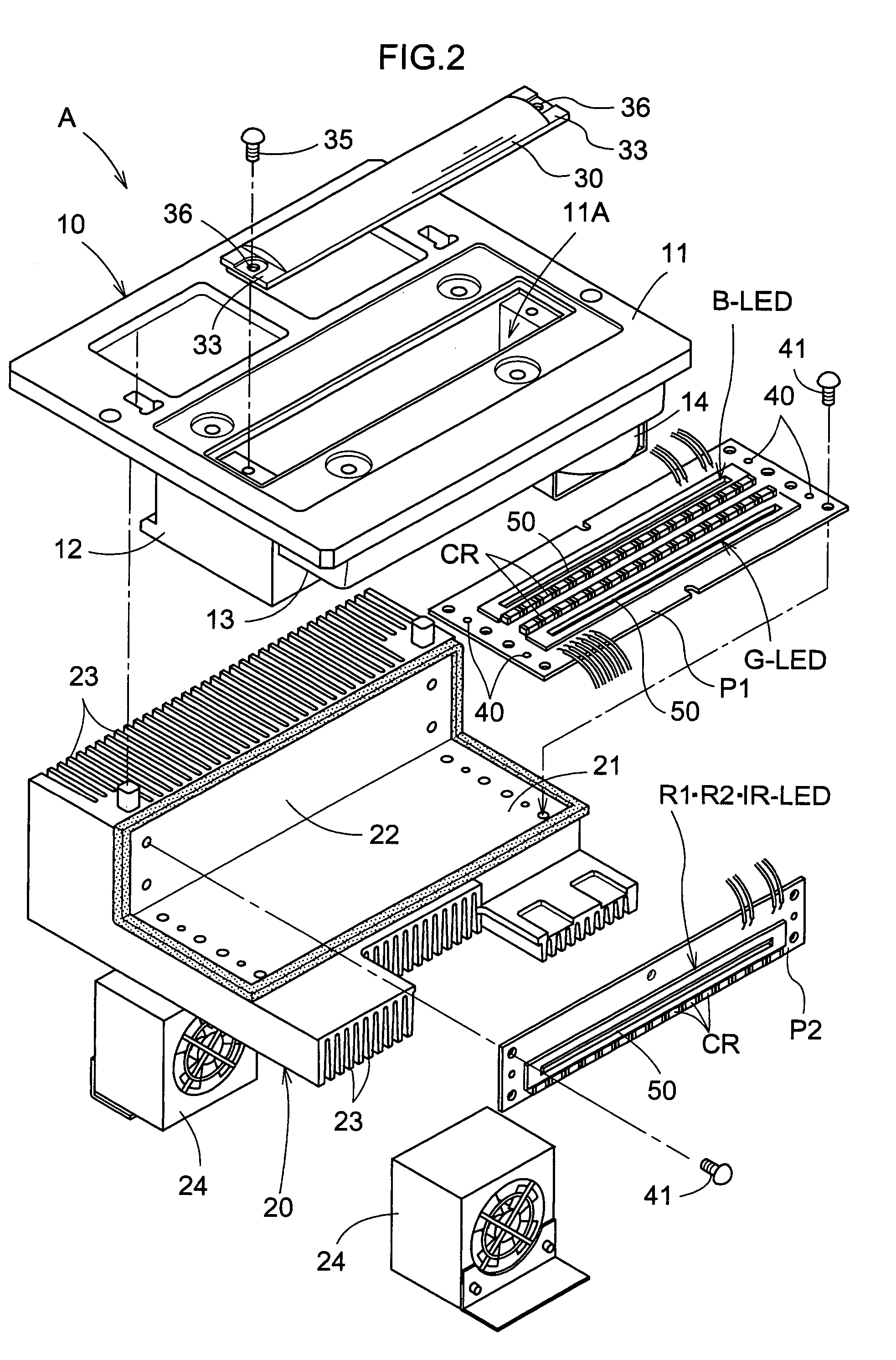
[0025]FIG. 1 shows an appearance of a film scanner using a light-emitting diode (LED) light source unit according to the present invention. This film scanner includes a light source unit A, a film carrier unit B, a lens unit C, a photoelectric converter unit D, and a control unit E. In operation, a beam from the light source unit A is irradiated on a developed photographic film F carried on the film carrier B and the transmission beam past this photographic film F is guided by the lens unit C to the photoelectric converter unit D. In this unit D, a CCD (Charge Coupled Device) type line sensor incorporated therein obtains, from an image in the photographic film F, image data in the form of digital signals corresponding to the three primary colors of R (red), G (green) and B (blue) and obtains also, by means of an infrared beam (IR), its beam intensity variable due to presence of a defect or flaw or dust or the like in the photographic film F as image data in the form of digital signa...


PUM


Abstract

A light-emitting diode (LED) light source unit includes a printed circuit board mounting LED elements thereon. The LED elements are arranged in the form of an array and mounted on a bottom face of a straight groove defined in the printed circuit board by a groove forming technique. A lateral face of the groove acts as a reflecting face for reflecting beam from the LED elements toward an object to be illuminated.

Description

FIELD OF THE INVENTION[0001]The present invention relates to a light-emitting diode light source unit including a printed circuit board mounting light-emitting diode elements.BACKGROUND OF THE INVENTION[0002]A light-emitting diode light source unit described above is employed as a light source for a facsimile machine, a scanner, etc. This unit has undergone various geometrical optics improvements for obtaining higher illumination intensity available therefrom. For instance, in the case of a light-emitting diode light source known from the Japanese Patent Application “Kokai” No.: Hei. 5-029665 (see paragraphs 0010–0013 and FIG. 2 thereof in particular), on a circuit board, there are arranged, in the form of an array, a plurality of light-emitting diode (LED) elements spaced apart along the length of the board and white resin portions are formed adjacent opposed ends of the array of the LED elements and a transparent resin portion is formed between the opposed white resin portions. Ea...

Claims


Application Information

Patent Timeline
Patent Type & Authority Patents(United States)
IPC IPC(8): F21V7/00G03B27/54B41J2/44F21K99/00F21S2/00F21S4/00F21V1/00F21V9/00F21V19/00F21V29/00F21Y101/02G02B27/00H01L25/075H01L31/12H01L33/58H01L33/60H01L33/62H04N1/028H04N1/04H05K1/02H05K1/05H05K1/18
CPCF21K9/00H01L33/60H04N1/02815H04N1/02865H05K1/0274F21V23/003H04N2201/0404H05K1/056H05K1/183H05K2201/09036H05K2201/09745H05K2201/10106H05K2201/2054H01L2224/48091H01L2224/4911H01L25/0753H01L2924/19107H01L2224/73265H01L2924/3011H01L2924/00014H01L2924/00
Inventor TAMAI, MASAYUKI
Owner NORITSU PRECISION CO LTD
Why Eureka
Try Eureka