Method for assembly of complementary-shaped receptacle site and device microstructures

a technology of complementary shapes and receptacle sites, applied in the field of assembly of hybrid electronic and optoelectronic circuits, can solve the problems of loose fit, difficult to produce complementary shapes between receptacles and device microstructures using this approach, and the method is typically limited to several microns of depth

Inactive Publication Date: 2006-03-28
HRL LAB
View PDF35 Cites 89 Cited by
  • Summary
  • Abstract
  • Description
  • Claims
  • Application Information

AI Technical Summary

Problems solved by technology

It is difficult to produce complementary shapes between receptacles and device microstructures using this approach because the microstructures require an exterior surface etch and the receptacles require an interior surface etch.
This leads to a loose fit.
This mismatch has been reported by other researchers in fluidic self-assembly.
These methods are typically limited to several microns of depth because the masking material and the polymer etch at the same rate.
Producing asymmetric receptacles (i.e. those with different sidewall profiles) is impractical using plasma etching.
Thus, forming receptacles by plasma etching for fluidic self-assembly applications is restricted to symmetric structures of limited depth.

Method used


Image

  • Method for assembly of complementary-shaped receptacle site and device microstructures
  • Method for assembly of complementary-shaped receptacle site and device microstructures
  • Method for assembly of complementary-shaped receptacle site and device microstructures

Examples


examples

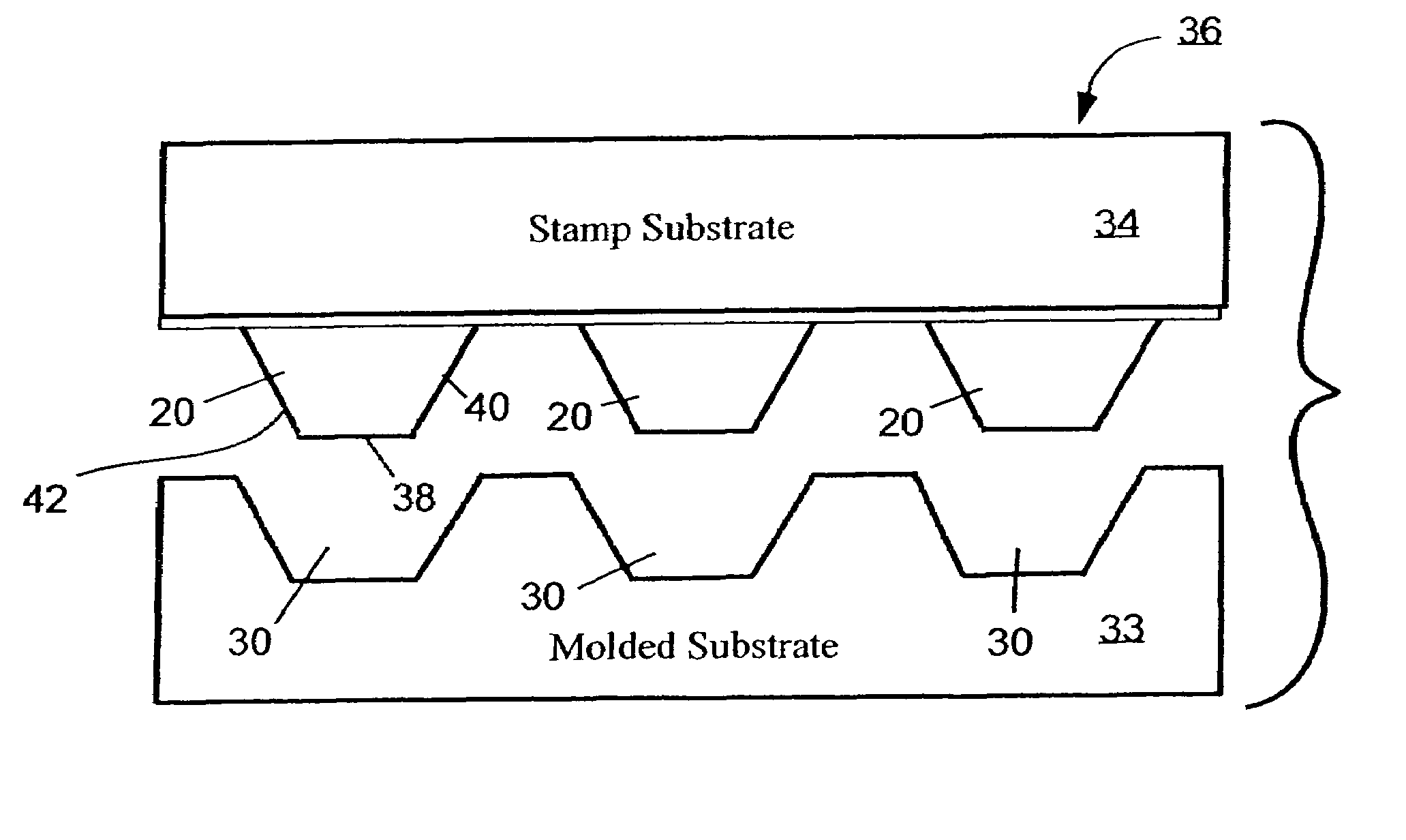
[0055]To show the operation of the invention, the inventors have assembled microstructure components into recesses formed in polymeric films using the method of the invention. FIG. 8 shows an array of receptacles formed in a polymer film by compression molding using this invention. The stamp used to form this impression was prepared from a silicon (100) wafer that was patterned using a wet-chemical (KOH) etch. The surface of the stamp was also treated chemically to allow easy release from the polymer after molding. This treatment involved making the silicon surface hydrophobic. This involved depositing a continuous Cr / Au film on the stamp surface and then forming an ordered organic monolayer (self-assembled monolayers, SAMS) on the Au surface. A detailed description of the preferred procedures used to fabricate the complementary shaped stamp and microstructures follows next.

[0056]With reference to FIG. 11, the device microstructures are fabricated using a commercially available sili...


PUM

PropertyMeasurementUnit
lengthaaaaaaaaaa
lengthaaaaaaaaaa
thicknessesaaaaaaaaaa

Abstract

A method for assembly including the steps of:(a) providing a plurality of microstructure components with each of the components having a bottom with the same three dimensional shape;(b) forming a mold with at least one protuberance from a surface thereof so that the at least one protuberance has the same shape;(c) molding a moldable substrate with the mold to form a molded substrate having a surface with at least one recess having the same shape; and(d) positioning a first of the plurality of microstructure components into said at least one recess. Each of the microstructure components may be formed by a masking and etching process, with the mold being formed by the same masking and etching process. The positioning step may consist of mixing the microstructure components with a fluid to form a slurry; and depositing the slurry on the surface of the molded substrate to cause the first of the plurality of microstructure components to self-align in the recess.

Description

CLAIM OF BENEFITS OF PROVISIONAL APPLICATION[0001]Applicants claim the benefits of their co-pending U.S. Provisional application Serial No. 60 / 326,055, filed on 28 Sept. 2001.FIELD OF INVENTION[0002]This invention relates to the assembly of hybrid electronic and optoelectronic circuits. In one embodiment, it involves a method for assembly of such circuits known as fluidic self-assembly.BACKGROUND OF INVENTION[0003]Fluidic self-assembly is a fabrication process whereby individual device microstructures are integrated into receptacle sites on host electronic circuits using a liquid medium for transport. Placement and registration of the device microstructures into receptacles on a substrate carrying electronic microcircuits is controlled by shape recognition or by selective chemical adhesion or both.[0004]Methods for fabricating device microstructures by fluidic self-assembly are known in the art. U.S. Pat. No. 5,545,291, which is incorporated herein by reference, describes one such m...

Claims


Application Information

Patent Timeline
Patent Type & Authority Patents(United States)
IPC IPC(8): H01L21/00B28B5/00B29C59/00H01L21/58H01L21/98H01L23/13H01L25/065H01L29/06
CPCB82Y10/00H01L23/13H01L24/26H01L24/83H01L24/95H01L25/0655H01L25/50B82Y30/00Y10T428/12528H01L29/0657H01L2224/8319H01L2224/8385H01L2224/95085H01L2924/01002H01L2924/01005H01L2924/01015H01L2924/01027H01L2924/01061H01L2924/01075H01L2924/01079H01L2924/01322H01L2924/07802H01L2924/09701H01L2924/10158H01L2924/10329H01L2924/14H01L2924/1423H01L2924/15153H01L2924/15157H01L2924/15165H01L2924/19041H01L2924/19042H01L2924/19043H01L2924/01006H01L2924/01019H01L2924/01024H01L2924/01033H01L2924/01072H01L2224/95145H01L2924/15787H01L2924/181H01L2224/95136H01L2924/00
Inventor BREWER, PETER D.HUNTER, ANDREW T.DECKARD, LUISA M.
Owner HRL LAB
Why Eureka
Try Eureka