Semiconductor memory device

a memory device and semiconductor technology, applied in the field of semiconductor memory devices, can solve the problems of unstable level of core voltage vcore, inability to supply a sufficient amount of current at a time, and unnecessary power consumption, and achieve the effect of preventing unnecessary power consumption and high data reliability

Inactive Publication Date: 2006-03-28
INTELLECTUAL DISCOVERY CO LTD
View PDF2 Cites 36 Cited by
  • Summary
  • Abstract
  • Description
  • Claims
  • Application Information

AI Technical Summary

Benefits of technology

[0024]It is, therefore, an object of the present invention to provide a semiconductor memory device that is capable of preventing unnecessary power consumption and providing high data reliability.

Problems solved by technology

However, due to the tendency of the low power consumption, it is difficult to supply a sufficient amount of the current at a time.
Therefore, a logic circuit for discharging the voltage level of the connection node to the desired level is required, resulting in the unnecessary power consumption.
In this case, if the activation width of the overdriving signal is short, the level of the core voltage VCORE is unstable even after the overdriving period.
Therefore, when a new active command is applied consecutively, data fail may be caused.
Because the conventional semiconductor memory device generates the overdriving signal having the constant activation pulse width without regard to the operation of the semiconductor memory device, the power may be dissipated unnecessarily and data fail may be caused.

Method used


Image

  • Semiconductor memory device
  • Semiconductor memory device
  • Semiconductor memory device

Examples


Embodiment Construction

[0033]Hereinafter, the present invention will be described in detail with reference to the accompanying drawings.

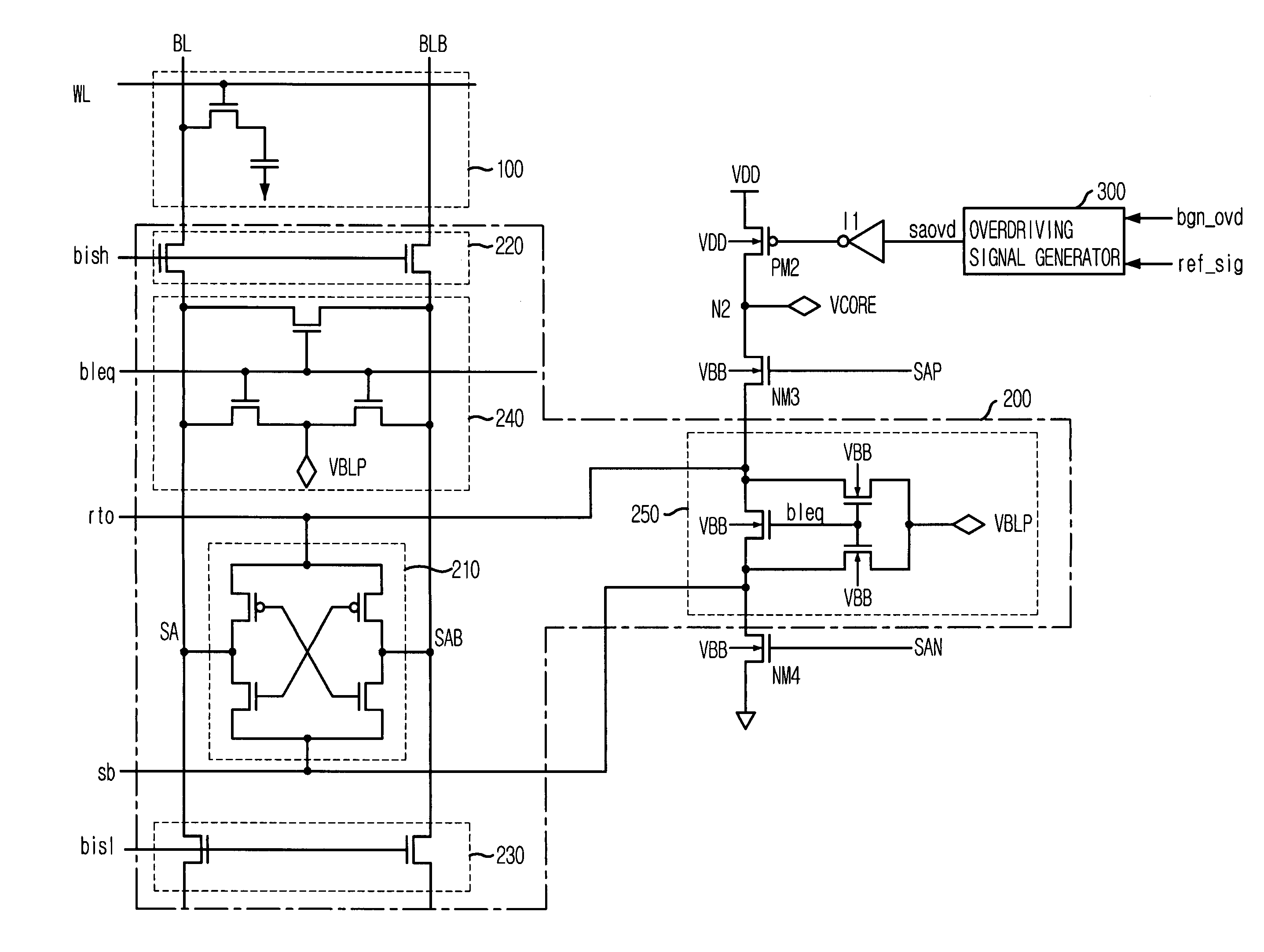
[0034]FIG. 4 is a circuit diagram of a semiconductor memory device having an overdriving structure in accordance with an embodiment of the present invention.

[0035]Referring to FIG. 4, the semiconductor memory device includes: a core voltage supplying part for supplying a core voltage; a memory cell array block 100; a bit line sense amplifier block 200 for sensing and amplifying a voltage difference of a bit line pair BL and BLB of the memory cell array block 100; an overdriving signal generator 300 for receiving an initial driving signal bgn_ovd to generate an overdriving signal saovd, while expanding an activation pulse width of the overdriving signal saovd in an activation of a refresh signal ref_sig; an overdriver PM2 for driving a connection node N2, which is coupled with the core voltage supplying part, to an external voltage VDD higher than the core voltage VCORE in...


PUM


Abstract

Provided is a semiconductor memory device that is capable of preventing unnecessary power consumption and providing high data reliability. The semiconductor memory device includes: a core voltage supplying part for supplying a core voltage; a memory cell array block; a bit line sense amplifier block for sensing and amplifying a voltage difference of bit line pairs of the memory cell array block; an overdriving signal generator for receiving an initial driving signal to generate an overdriving signal, while expanding an activation pulse width of the overdriving signal in an activation of a refresh signal; an overdriver for driving a connection node, which is coupled with the core voltage supplying part, to an external voltage higher than the core voltage in response to an inverted overdriving signal; a first power driver for driving a first power line of the bit line sense amplifier block to a voltage of the connection node in response to a first driving control signal; and a second power driver for driving a second power line of the bit line sense amplifier to a first power voltage in response to a second driving control signal.

Description

FIELD OF THE INVENTION[0001]The present invention relates to a semiconductor design technology; and, more particularly, to a semiconductor memory device for adjusting a driving force of an overdriver.DESCRIPTION OF RELATED ART[0002]As a low driving voltage is used for the purpose of low power consumption, a semiconductor memory device including a dynamic random access memory (DRAM) uses various circuits for helping an operation of a sense amplifier. One of them is an overdriving structure of a sense amplifier.[0003]In general, data from a plurality of memory cells connected to a word line activated by a row address are transferred to a bit line and a bit line sense amplifier senses and amplifies a voltage difference of a bit line pair.[0004]In the above operation, thousands of bit line sense amplifiers start to operate at the same time. Therefore, a driving time of the bit line sense amplifier is determined according to whether a sufficient amount of a current for driving it can be ...

Claims


Application Information

Patent Timeline
Patent Type & Authority Patents(United States)
IPC IPC(8): G11C7/00
CPCG11C7/06G11C11/406G11C29/50012G11C11/4091G11C29/02G11C29/028G11C11/4074G11C11/401
Inventor LEE, SANG-HEE
Owner INTELLECTUAL DISCOVERY CO LTD
Why Eureka
Try Eureka