Printed circuit board trace routing method

a technology of printed circuit boards and routing methods, which is applied in the field of routing traces on printed circuit boards, can solve the problems of difficult to predict the signal propagation speed along the trace, the relative position of the relative positions of the relative positions of the relative positions, and the possibility of impedance variations between the traces

Inactive Publication Date: 2006-04-04
INTEL CORP
View PDF4 Cites 72 Cited by
  • Summary
  • Abstract
  • Description
  • Claims
  • Application Information

AI Technical Summary

Problems solved by technology

Even when a trace runs over a glass strand, their relative positions may change, due to a skewing of the underlying glass strands.
These varying conditions make it difficult to ascertain the dielectric constant of the PCB beneath the trace, thus making the signal propagation speed along the trace difficult to successfully predict....

Method used


Image

  • Printed circuit board trace routing method
  • Printed circuit board trace routing method
  • Printed circuit board trace routing method

Examples


Embodiment Construction

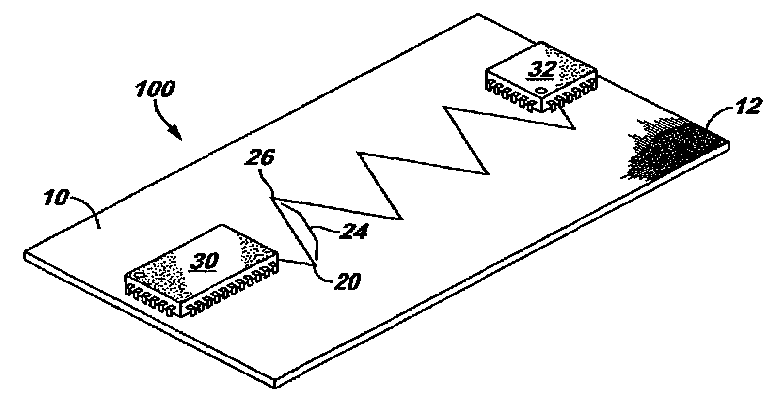
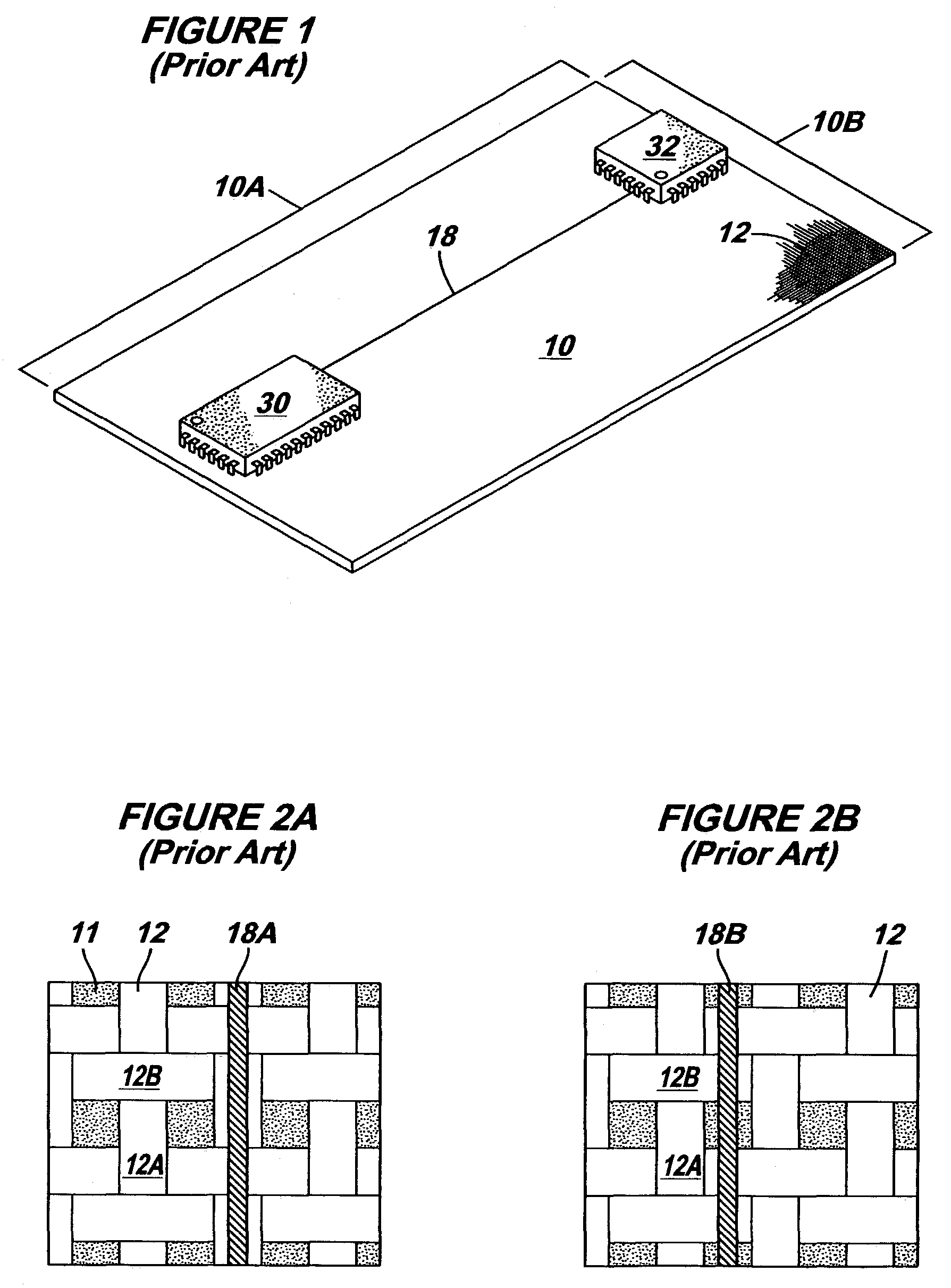
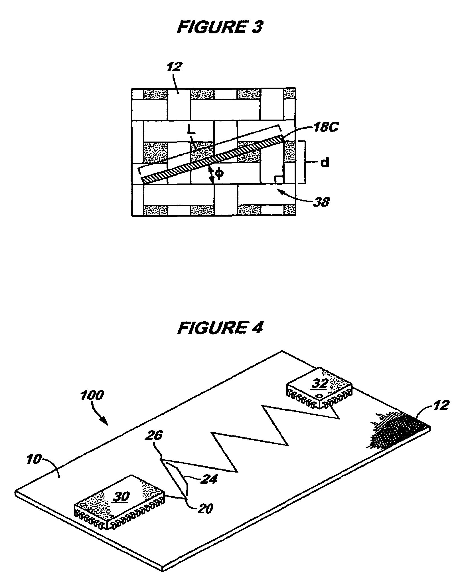
[0021]In accordance with some embodiments described herein, an I / O routing pattern method is disclosed, for use with heterogeneous printed circuit boards (PCBs), such as those embedded with a reinforcement material, for example, a fiberglass weave. Traces are routed on the PCB so as to reduce sensitivity to changes in the dielectric constant (Dk), which are brought about by the strands of reinforcement material contained within the PCB laminate. The method minimizes the impact of local variations, such as the Dk, time of flight, and capacitance variations, that are observed with traditional routing methods on heterogeneous PCBs.

[0022]In some embodiments, traces are routed between circuits on the PCB in a zig-zag pattern, such that multiple strands of reinforcement material are disposed beneath each portion of the zig-zag trace. The strands are embedded into the PCB in a known manner, such as with an FR-4-type PCB, in which glass strands are aligned at right angles to one another in ...


PUM

PropertyMeasurementUnit
Lengthaaaaaaaaaa
Capacitanceaaaaaaaaaa
Dielectric constantaaaaaaaaaa

Abstract

An I/O routing pattern method is disclosed, for use with heterogeneous printed circuit boards (PCBs), such as those embedded with a reinforcement material, for example, a fiberglass weave. Traces are routed on the PCB so as to reduce sensitivity to changes in the dielectric constant (Dk), which are brought about by the strands of reinforcement material contained within the PCB laminate. The method minimizes the local variations, such as the Dk, time of flight, and capacitance variations, that are observed with traditional routing methods on heterogeneous PCBs.

Description

FIELD OF THE INVENTION[0001]This invention relates to printed circuit boards and, more particularly, to techniques for routing traces on printed circuit boards.BACKGROUND OF THE INVENTION[0002]Printed circuit boards (PCBs), also known as printed wiring boards, are used to interconnect and assemble electronic circuits. The operating temperature, mechanical strength, and other characteristics of a PCB, may vary according to the application in which the PCB is used. PCBs provide electrical conductor paths between the circuits disposed upon them.[0003]Some PCBs consist of paper or woven glass impregnated with an epoxy resin. PCBs may include materials such as copper, iron, aluminum, or ceramic. Flexible PCBs may have polyester or polyimide bases. Ultimately, PCBs typically include at least a resin-based material, a reinforcement material, and one or more conductive foils.[0004]FR-4 is the most common printed circuit board material, and is used in the majority of computer-based applicati...

Claims


Application Information

Patent Timeline
IPC IPC(8): H05K1/16H05K1/02H05K1/03
CPCH05K1/0248H05K1/0366H05K1/025H05K1/0245H05K2201/09263H05K2201/029
Inventor BRIST, GARY A.LONG, GARY B.ALGER, WILLIAM O.MILLER, DENNIS J.
Owner INTEL CORP
Why Eureka
Try Eureka