

Integrated circuit devices having dielectric regions protected with multi-layer insulation structures
a technology of integrated circuit memory and dielectric layer, which is applied in the direction of semiconductor devices, capacitors, electrical devices, etc., can solve the problems of reducing the reliability of resultant devices, complex manufacturing process associated with forming such capacitors, and the dielectric characteristic of the dielectric layer can be degraded during the manufacturing of integrated circuit memory devices, so as to reduce the diffusion of hydrogen
- Summary
- Abstract
- Description
- Claims
- Application Information
AI Technical Summary
Benefits of technology
Problems solved by technology
Method used
Image

Examples
second embodiment
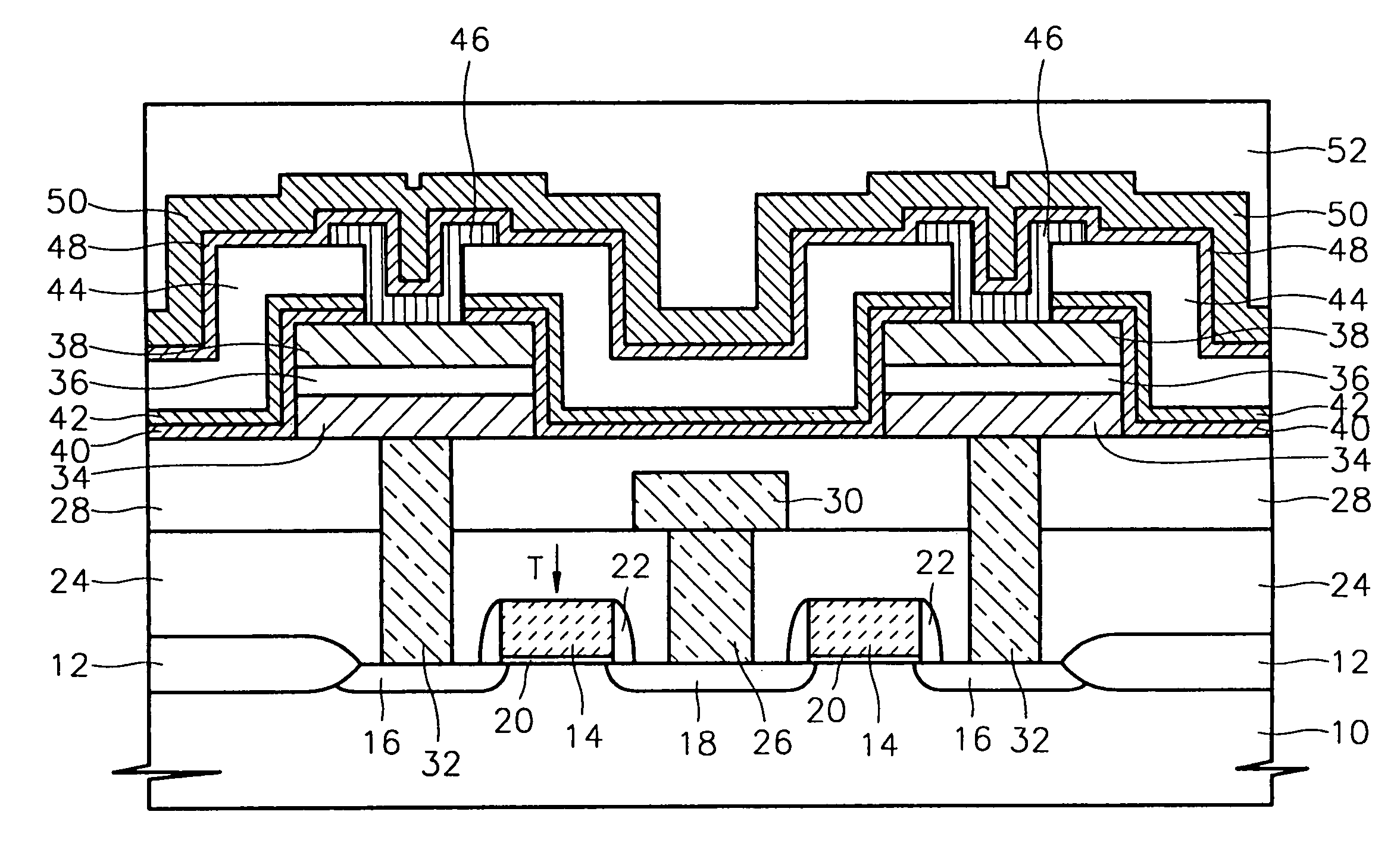
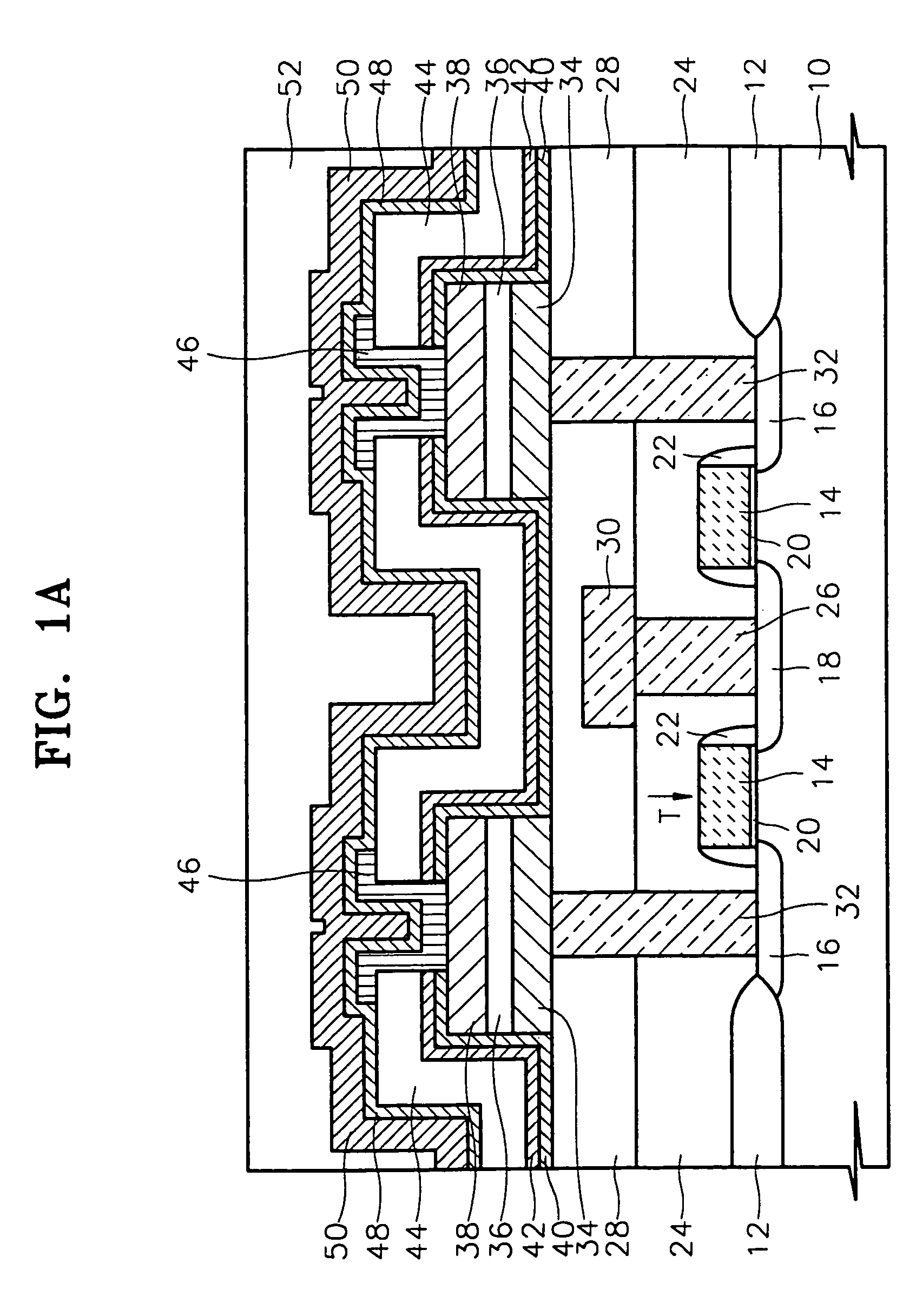
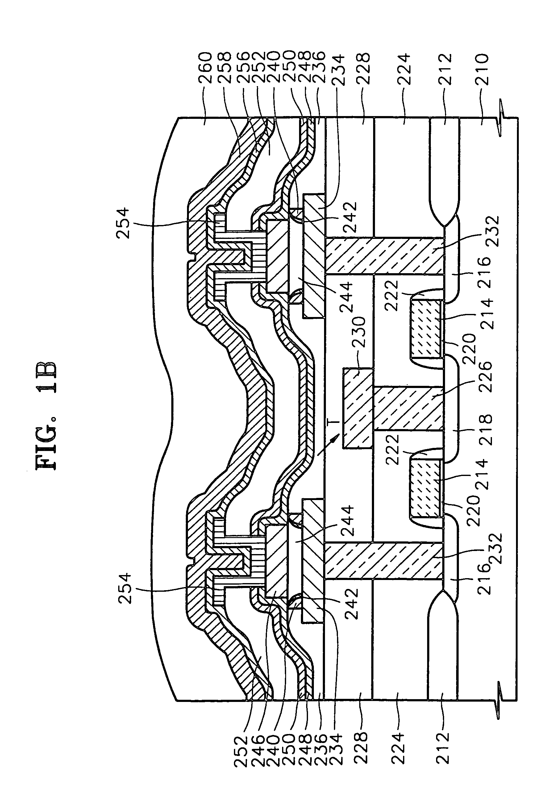
[0032]FIG. 1B is a sectional view illustrating the structure of a memory device according to the present invention. A semiconductor substrate 210, a device isolation layer 212, transistors 214, 216, 218, 220 and 222, a first interlayer insulation layer 224, a landing plug 226, a second interlayer insulation layer 228, a bit line contact pad 230, a contact plug 232 and a lower electrode 234 of a capacitor are substantially the same as the semiconductor substrate 10, the device isolation layer 12, transistors 14, 16, 18, 20 and 22, the first interlayer insulation layer 24, the landing plug 26, the second interlayer insulation layer 28, the bit line contact pad 30, the contact plug 32 and the lower electrode 34 of a capacitor illustrated in FIG. 1A.
[0033]A dielectric layer 244 is formed at the center of the top surface of the lower electrode 234 of a capacitor. A third interlayer insulation layer 236 extends from one end of the lower electrode 234 of a capacitor to one end of an adjace...
first embodiment
[0038]Methods for determining the thicknesses of and the annealing temperatures for the protection layer 250 and blocking layer 248 of the first encapsulating layer, the protection layer 258 and blocking layer 256 of the second encapsulating layer, the protection spacer 242 and the blocking spacer 240, are similar to those described in the
[0039]Compared to the embodiment of FIG. 1A, this embodiment further forms the protection spacer 240 for reducing the diffusion of hydrogen generated during later processes (processes of forming interlayer insulation layers) and the blocking spacer 242 for reducing the diffusion of hydrogen generated during the formation of the protection spacer 240, on each sidewall of the dielectric layer 244, thereby more effectively reducing the diffusion of hydrogen generated during semiconductor manufacturing processes.
[0040]A method of forming the semiconductor device of FIG. 1A will be described with reference to FIGS. 2A through 2C.
[0041]Referring to FIG. ...
PUM
 Abstract
Description
Claims
Application Information