

Semiconductor device including nonvolatile memory
a non-volatile memory and semiconductor technology, applied in the direction of semiconductor devices, electrical appliances, transistors, etc., can solve the problems of complicated device structure of circuits and logic circuits
- Summary
- Abstract
- Description
- Claims
- Application Information
AI Technical Summary
Benefits of technology
Problems solved by technology
Method used
Image

Examples
first embodiment
[0021]the invention is hereinafter explained.
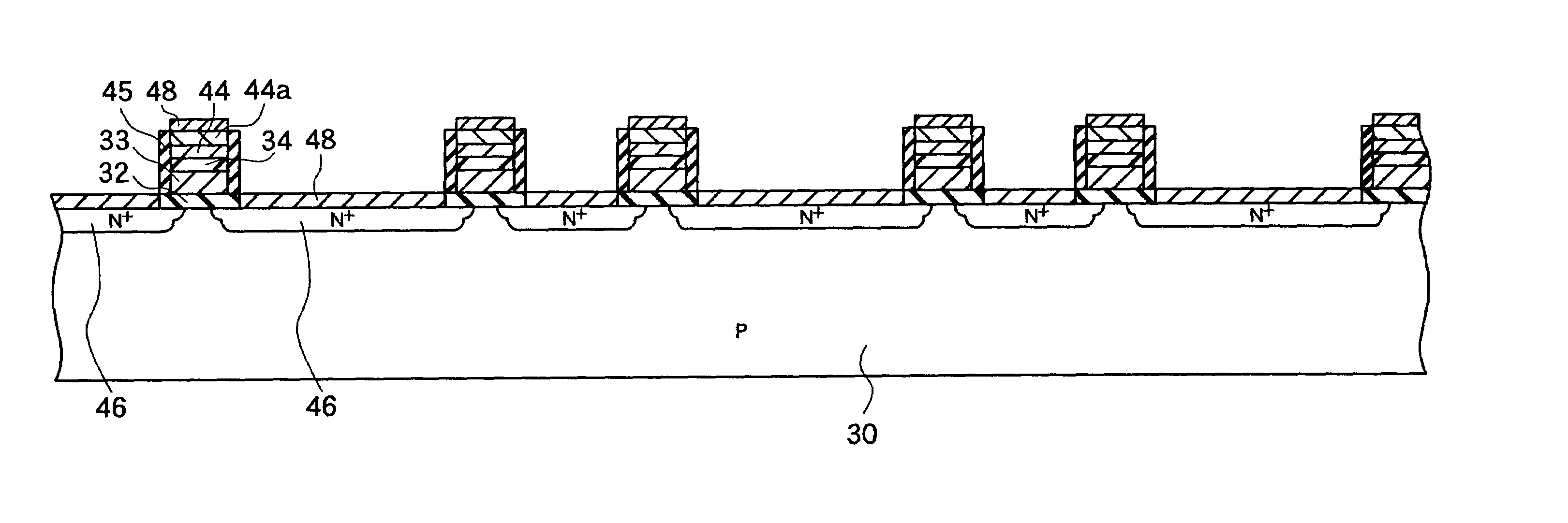
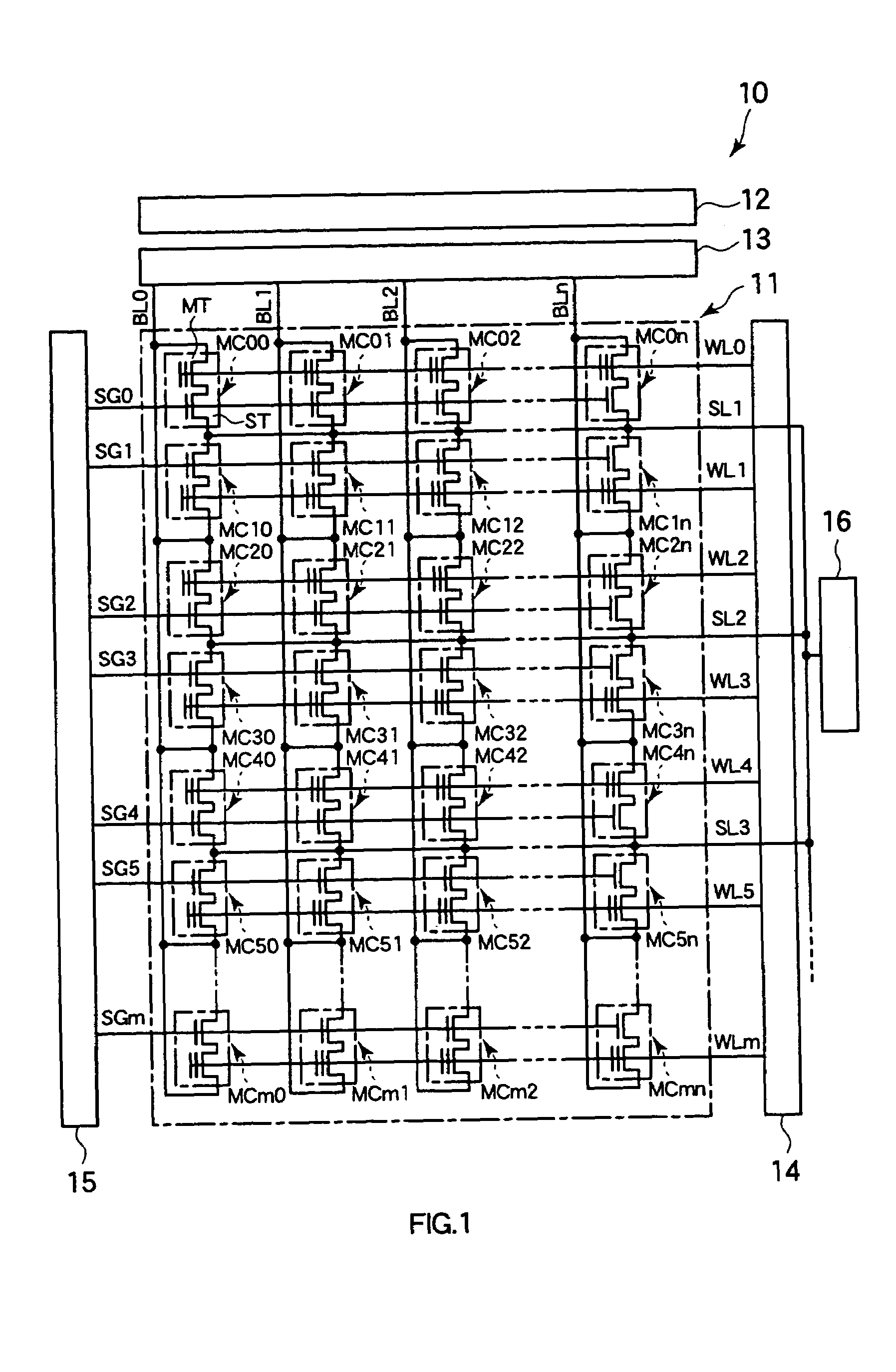
[0022]A nonvolatile memory of the first embodiment is a flash memory having a memory cell formed of two first MOS transistors.
[0023]The first MOS transistor has a first gate of a layered structure. The layered structure includes a first insulating film for a tunnel insulating film, a first gate electrode film for a floating gate electrode film, a second gate insulating film for an inter-gate insulating film and a second gate electrode film for a control gate electrode film.
[0024]On the other hand, a logic circuit of the first embodiment includes a periphery circuit. The logic circuit contains a CMOS logic circuit having second MOS transistors. Each of the second MOS transistors has a second gate, which is a layered structure of a third gate insulating film and the second gate electrode film.
[0025]Moreover, the third gate insulating films of the second MOS transistors have three kinds of different film thicknesses respectively. Each of the...
second embodiment
[0080]present invention is hereinafter explained.
[0081]The basic structure of a second embodiment of this invention is almost the same as that of the first embodiment. A different point from the first embodiment is a point that the second embodiment has a third gate electrode film in the gate structure. The third gate electrode film is stacked on the second gate electrode film in the gate structure.
[0082]A nonvolatile memory in the second embodiment is a flash memory having a memory cell formed of two first MOS transistors.
[0083]The first MOS transistor has a first gate of a layered structure. The layered structure includes a first insulating film for a tunnel insulating film, a first gate electrode film for a floating gate electrode film, a second gate insulating film for an inter-gate insulating film, a second gate electrode film and a third gate electrode film for a control gate electrode film.
[0084]On the other hand, a logic circuit includes a periphery circuit. The logic circui...
third embodiment
[0113]present invention is hereinafter explained
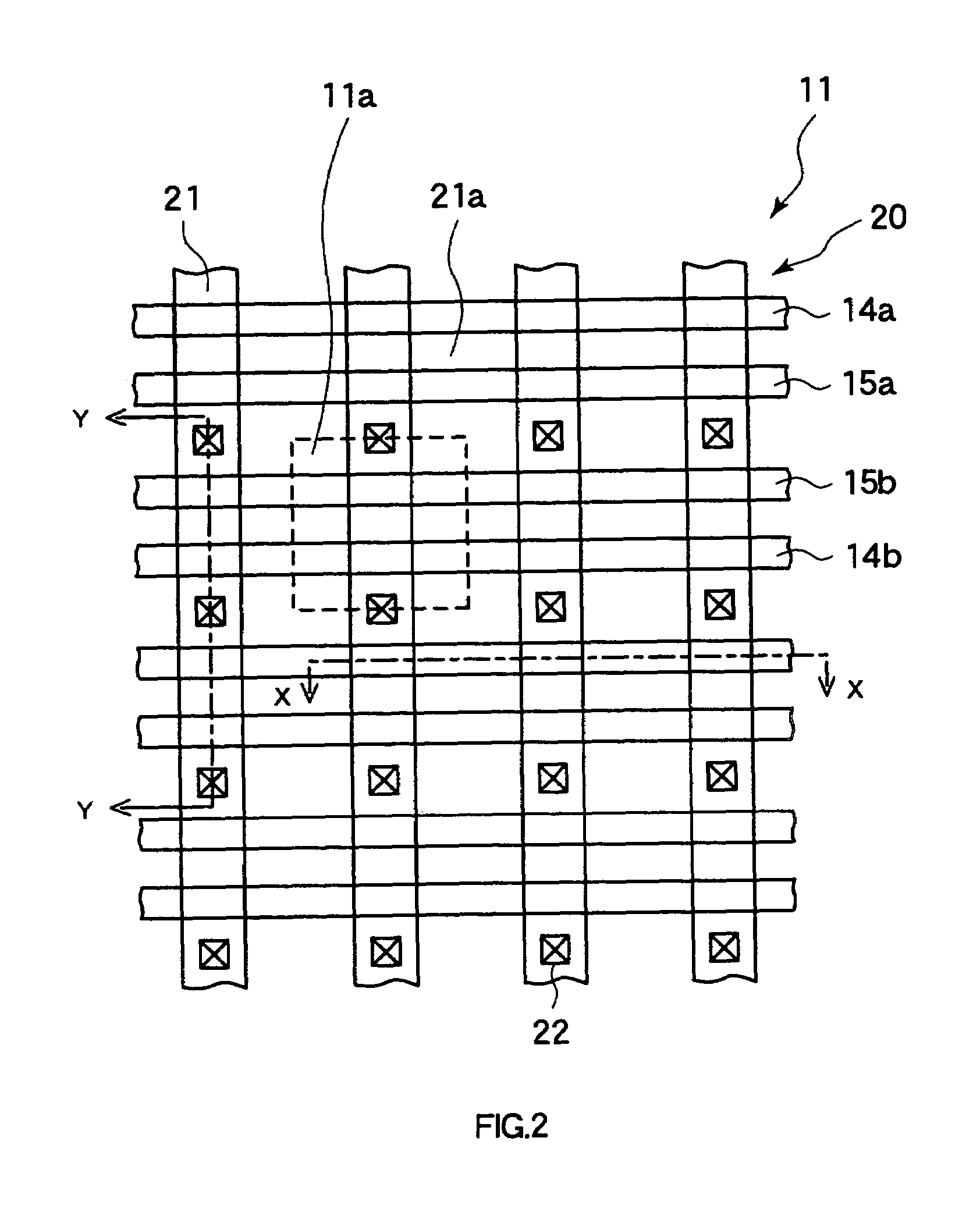
[0114]FIG. 6 shows a block diagram of a system LSI in the third embodiment of the present invention. The third embodiment is a system LSI including a plurality of nonvolatile memory circuits.
[0115]The system LSI 50 has a logic circuit area 50a and a memory area 50b. For example, CPU 51 is formed in logic circuit area 50a. Three kinds of nonvolatile memories are formed in memory area 50b. Three kinds of nonvolatile memories are nonvolatile memory 10 having a memory cell unit formed from two transistors explained in the first embodiment and the second embodiment above-mentioned, NAND-type nonvolatile memory 10a and nonvolatile memory 10b having a memory cell unit formed of the three transistors.
[0116]In system LSI 50, nonvolatile memory 10 having a memory cell unit formed of two transistors and CPU 51 are included in the same chip, so nonvolatile memory 10 can be used as a read-only memory, which stores the firmware of CPU 51.
[0117]The c...
PUM
 Abstract
Description
Claims
Application Information