Design-manufacturing interface via a unified model

a design-manufacturing interface and unified model technology, applied in the field of integrated circuits, can solve the problems of insufficient reproduction of geometrical shapes on masks, increasing challenges to the semiconductor industry by cd miniaturization, and increasing tension in ic fabrication

Active Publication Date: 2005-04-07
SYNOPSYS INC
View PDF4 Cites 195 Cited by
  • Summary
  • Abstract
  • Description
  • Claims
  • Application Information

AI Technical Summary

Problems solved by technology

The CD miniaturization trend increasingly challenges the semiconductor industry.
IC fabrication is increasingly strained with decreasing CDs from one technology generation to the next.
The geometrical shapes on masks are not reproduced properly onto the wafer.
This phase difference causes destructive interference, thus creating sharp images between the regions.
But the use of these techniques can necessitate so much layout modification that the modified layout has little resemblance to target wafer shapes.
In addition to low-k1 imaging artifacts, decrease in focus tolerance is another issue for optical lithography.
Left unattended, wafer topography can cause difficulties for photolithography because of DoF issues.
This increased pressure translates to polishing rate increase, causing non-uniformity in the removal rate across patterns of different pattern densities.
The layout modification steps illustrated in FIG. 10 generally add many shapes to the layout data, thereby increasing data volume and mask cost.
Some of the added shapes may affect mask manufacturability and yield.
Although the virtual stepper technique evaluates the lithography impact of mask anomalies, it cannot assess their electrical impact.
The IC creation flow illustrated in FIG. 1 and FIG. 10 is becoming inadequate with CD miniaturization.
Associated with increasing manufacturing complexity is a drastic increase in the number of design rules for each technology.
Definition, maintenance, and verification of design rules have become a time-consuming, resource-intensive, and error-prone process.
Moreover, design rules inherently lack satisfactory two-dimensional descriptions.
The large number of design rules is thus still insufficient in capturing all subtleties of advanced fabrication processes and nano-scale phenomena.
Similar difficulties with rules have been encountered in OPC, where the industry has witnessed a switch from rule-based to model-based OPC implementations.
But these rules are generally relaxed compared with the normal rule set such that implementation of these preferred design rules diminishes performance, for example, by reducing circuit density, and decreases silicon efficiency.
Moreover, there is a discrepancy in fineness of control between design rules and layout modification such as OPC.
Such discrepancy means that the fineness gained by one can be lost by the coarseness of the other.
Another issue with design rules concerns design rule migration.
A low-quality design rule may be incorporated during this initial definition phase and results in layouts that have inferior manufacturability.
They need to be fixed at such an early stage because the time it takes to design a circuit, to develop mature processes, and to establish design rules make the IC creation process rather rigid.
Design rules once established are very difficult to change.
Using these fixed design rules, circuit designers cannot take advantage of possible improvements afforded by later process changes.
Becoming more apparent with advances in semiconductor technology, design rule inadequacies are resulting in slack and inefficiencies in the IC creation process.
Design rules is becoming a limiting factor in the IC creation flow.
In addition to affecting DRC and confidence in the manufacturability of layouts, design rule inadequacies also have ramifications on all parts of the IC creation flow where design rules are used.
A router that uses the drawn square shapes and constrained by the design rule [s (1106)] would not be able to make this direction connection, a route that decreases wire length and potentially reduces circuit area.
Shape distortion arising from the fabrication process can also affect circuit extraction.
Since the delineated shapes on the wafer are different from the layout shapes, circuit information extracted from the layout shapes such as parasitic capacitance, inductance, and resistance can be insufficient for performance verification.
Segregation is another drawback of the data modification steps.
Such segregation can result in superfluous data modification.

Method used


Image

  • Design-manufacturing interface via a unified model
  • Design-manufacturing interface via a unified model
  • Design-manufacturing interface via a unified model

Examples


Embodiment Construction

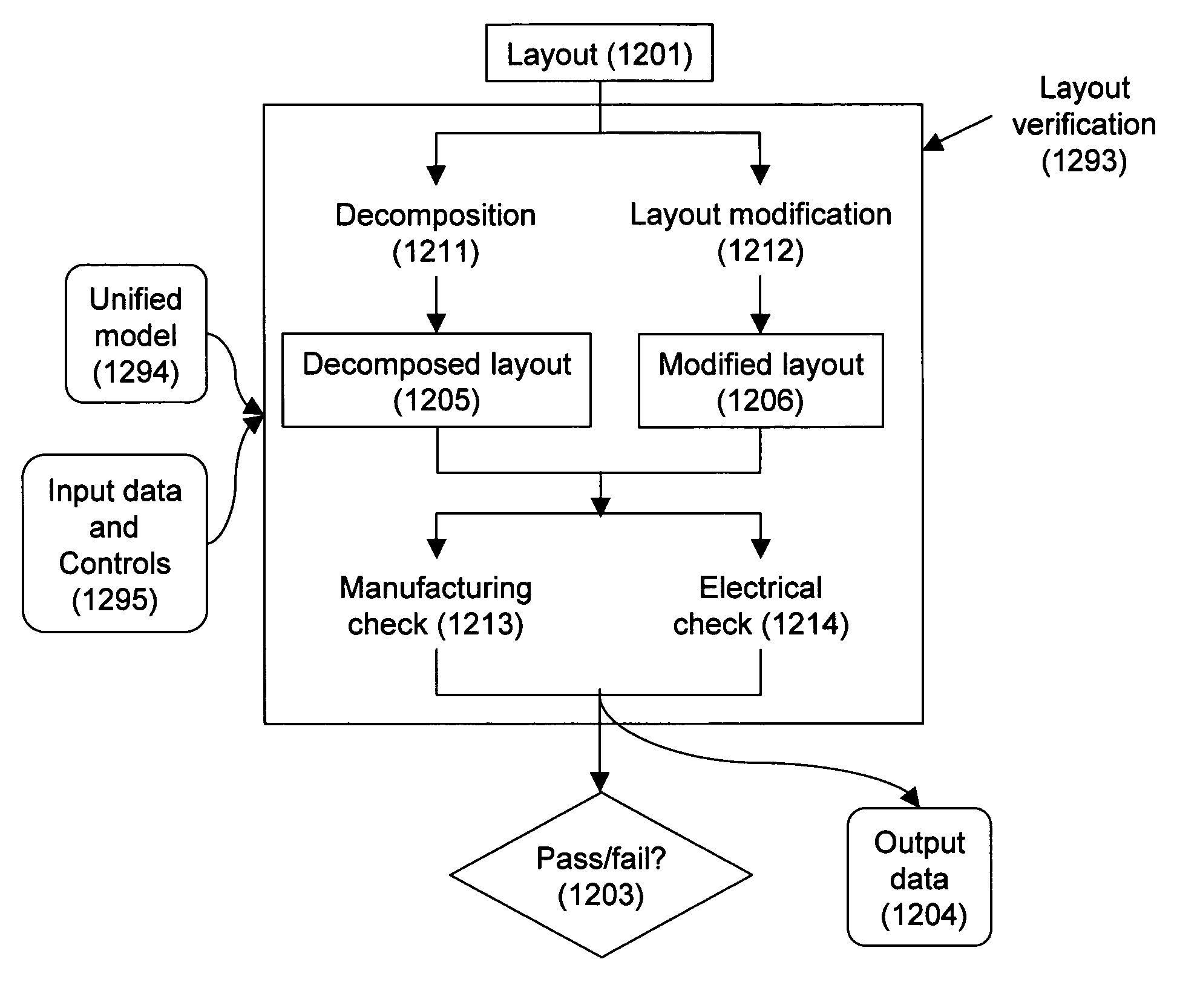
To address the issues with existing design rules and to maintain the advantage of design-manufacturing division, the layout verification process shown in FIG. 12 has been developed to complement or to replace the existing DRC process shown in FIG. 2. Given a layout (1201) representing target wafer shapes or shapes from which target wafer shapes can be derived, a unified model of manufacturing processes and circuit elements (1294), and input data and controls (1295), layout verification (1293) determines whether the layout shapes are properly sized and placed such that the circuit eventually fabricated is both manufacturable and electrically functional. The input data and controls (1295) can provide the layout verification process (1293) with information including the specifics of the layout such as the prime cell name, the layout data format, and the layer mapping information. They can also control layout verification (1293), for example, by specifying the layout levels to be verif...


PUM


Abstract

Subtleties of advanced fabrication processes and nano-scale phenomena associated with integrated circuit miniaturization have exposed the insufficiencies of design rules. Such inadequacies have adverse impact on all parts of the integrated circuit creation flow where design rules are used. In addition, segregation of the various layout data modification steps required for deep sub-micrometer manufacturing are resulting in slack and inefficiencies. This invention describes methods to improve integrated circuit creation via the use of a unified model of fabrication processes and circuit elements that can complement or replace design rules. By capturing the interdependence among fabrication processes and circuit elements, the unified model enables efficient layout generation, resulting in better integrated circuits.

Description

FIELD OF THE INVENTION This invention relates to the creation of integrated circuits. More specifically, the invention relates to an efficient and efficacious interface between design and manufacturing that improves the quality of information transfer from design to manufacturing and from manufacturing to design. Such improvement enhances the quality of the chips manufactured. RELATED ART An integrated circuit (IC) is a piece of hardware that processes data. A representative IC creation flow is depicted in FIG. 1. From a high-level functional description such as speed of operation, footprint, power consumption, and input-output (I / O) of the chip, representation of the IC is refined progressively, with lower-level details being added in each step until the physical IC chip is made. The flow comprises design and manufacturing as the two primary aspects, which are shown respectively in FIG. 1a and FIG. 1b. Starting from the design aspect illustrated in FIG. 1a, some of the functiona...

Claims


Application Information

Patent Timeline
Patent Type & Authority Applications(United States)
IPC IPC(8): G06F17/50
CPCG06F17/5036G06F17/5081G06F17/5068G06F30/367G06F30/39G06F30/398
Inventor PIERRAT, CHRISTOPHEWONG, ALFRED KWOK-KIT
Owner SYNOPSYS INC
Why Eureka
Try Eureka